Chinese Firm to Open UK Chip R&D Center

发布时间:2018-02-11 00:00
作者:Ameya360
来源:Nitin Dahad
阅读量:930

  LONDON — The China-based parent company of Dynex Semiconductor is establishing a semiconductor R&D center in the UK. The center will employ up to 200 engineers over the next three years and provide additional research capability for its CRRC's two UK subsidiaries, Dynex and Soil Machine Dynamics.

  CRRC Times Electric, a Chinese developer of rail and electric vehicle control systems, said it plans to establish the Times Electric Innovation Centre (TEIC) in the first half of 2018 in Birmingham, England. It will focus on cutting-edge research and development of semiconductor-based products and technology across a wide power range. This research will be applicable to key growth markets, including electric vehicles, rail traction, aerospace, power distribution and renewable energy, the firm said.

  The TEIC is part of the strategy for a combined CRRC Times Electric and Dynex partnership to become a major global player in semiconductor technology. Dynex and Soil Machine Dynamics will have full, royalty-free, access to relevant semiconductor-related outputs of the new TEIC.

  Dynex is headquartered in the city of Lincoln, in England's East Midlands region, where it plans to continue conducting R&D. In the last 12 months, Dynex has been heavily focused on new product such as its trench gate and DMOS high-power IGBT modules, press-pack IGBTs, new HVDC products, and the launch of its new foundry services business. The Lincoln R&D center expects to have more new product releases in the coming months from Dynex.

  "The TEIC will have significant capabilities in semiconductor innovation, as well as other power electronics and related systems," said Clive Vacher, Dynex president and CEO. "It will support Dynex, SMD, and all CRRC entities.  Over time, its capabilities will develop in several different directions and will not be limited to high-power semiconductors."

(备注:文章来源于网络,信息仅供参考,不代表本网站观点,如有侵权请联系删除!)

在线留言询价

相关阅读
Chip-on-Board (COB) vs. Package-on-Package (PoP)- Comparison and Applications
  The ever-evolving landscape of electronic devices demands innovation in packaging technologies. Among the array of approaches available, two prominent methods stand out: Chip-on-Board (COB) and Package-on-Package (PoP). These techniques play pivotal roles in the assembly, functionality, and miniaturization of electronic components, each with distinct advantages and applications.  Chip-on-Board (COB)  COB is a packaging technique that involves mounting bare semiconductor chips directly onto a substrate or a Printed Circuit Board (PCB). This method eliminates the use of individual packaging for each chip, opting instead for direct bonding or soldering onto the board’s surface. By doing so, COB reduces space requirements and enhances heat dissipation efficiency.  One of COB’s key strengths lies in its compactness. By eschewing traditional packaging, this approach significantly reduces the overall size of electronic devices, making it ideal for applications where space is a constraint. Moreover, the direct connection between the chip and the substrate minimizes signal interference, enhances electrical performance, and reduces circuit inductance and resistance.  COB technology finds widespread use across various industries. In automotive applications, COB is often utilized in LED lighting modules, offering higher brightness levels and superior thermal management due to the close arrangement of LED chips. Additionally, COB’s cost-effectiveness makes it appealing for applications where simplicity in circuitry is essential.  Package-on-Package (PoP)  In contrast to COB, Package-on-Package (PoP) involves vertically stacking multiple packaged chips within a single device. This configuration enables the integration of different functionalities or components, such as memory and processors, into a compact assembly. The stacking of chips facilitates enhanced performance without increasing the device’s footprint.  PoP’s primary advantage lies in its versatility. By vertically stacking chips, PoP allows for better integration of various components, leading to improved performance and reduced signal distortion due to shorter interconnection paths. This technology excels in accommodating diverse functionalities within limited space, making it a preferred choice for applications where performance and miniaturization are critical factors.  Mobile devices, particularly smartphones and tablets, heavily leverage PoP technology. These devices require high-performance capabilities within a confined space. PoP facilitates the integration of memory chips and processors, enabling seamless multitasking and high-speed data transfer without compromising on performance.  Chip-on-Board (COB) vs. Package-on-Package (PoP)- Comparison and ApplicationsWhen weighing the advantages of COB and PoP, the choice between the two largely depends on specific design requirements and application needs. COB’s strengths in compactness, cost-effectiveness, and thermal management make it suitable for applications where space optimization and simplicity in circuitry are crucial.  Conversely, PoP’s versatility in accommodating multiple functionalities within a confined space makes it ideal for devices requiring high performance without sacrificing miniaturization. Industries such as mobile technology heavily rely on PoP to enhance the capabilities of their devices while maintaining a compact form factor.  ConclusionBoth Chip-on-Board (COB) and Package-on-Package (PoP) are indispensable packaging technologies in the realm of modern electronics. Understanding their differences enables manufacturers and designers to make informed decisions based on specific requirements, contributing to the development of innovative and efficient electronic devices catering to diverse consumer needs.  By harnessing the capabilities of COB and PoP, the electronics industry continues to evolve, providing consumers with increasingly powerful yet compact devices across various applications, from consumer electronics to automotive and beyond.
2024-03-21 16:32 阅读量:601
What types of chip packaging substrates are there?
  In the field of semiconductor packaging, many packaging types use packaging substrates, such as BGA (Ball Grid Array), PGA, QFP, CSP, SiP, PoP, etc. Different types of packaging use different packaging substrates. So what are the common packaging substrates? Keep reading!  What is the function of packaging substrate?  The packaging substrate has the following main functions in the package: electrical connection, mechanical support, heat dissipation, protection, etc.  What types of packaging substrates are there?  According to the material of the substrate, it is divided into rigid substrate and flexible substrate.  Rigid substrate refers to a substrate that has strong rigidity and cannot be bent. Flexible substrates refer to substrates that can be bent and folded. Rigid substrates have a fixed shape and form, while flexible substrates are thin and more flexible.  What type of material is the rigid substrate made of?  Common rigid substrate materials: FR4, BT, ABF, ceramic, etc.  FR4  FR4 is one of the most commonly used material types in printed circuit board (PCB) manufacturing. “FR4” stands for “Flame Retardant Type 4”. It is a composite material made of fiberglass cloth impregnated with epoxy resin, then hot pressed and cured. It has the characteristics of good flame retardancy, high mechanical strength, excellent electrical insulation performance and good thermal stability.  BT  BT material, which takes its name from its main chemical components: Bismaleimide and Triazine, is a more advanced and higher-performance epoxy resin substrate and has become the lamination of choice for many substrate manufacturers. BT material has a high glass transition temperature, usually higher than ordinary FR4 materials; low thermal expansion coefficient and dielectric constant; good insulation, etc. BT is the standard substrate material for BGA packages and can also be used for CSP packages.  ABF  ABF (Ajinomoto Build-up Film) is a highly rigid and highly durable material used in high-end chip packaging such as CPUs and GPUs. It was developed by Ajinomoto Company. It is a laminated film material and is usually used as an inner insulating material for packaging substrates.  Ceramics  Commonly used ceramic materials include aluminum oxide (Al2O3), aluminum nitride (AlN), beryllium oxide (BeO), silicon carbide (SiC), etc., which are relatively early laminated materials. Ceramic materials are first obtained in the form of powder through grinding to obtain particles of suitable particle size, and then are made through shaping, metallization, lamination, cutting, high-temperature sintering, grinding and polishing, nickel immersion, gold immersion, etc. They have a certain degree of brittleness and are suitable for high-frequency applications in chip products with high power and high reliability requirements.  What types of materials are used for flexible substrates?Common flexible substrate materials: PI (polyimide), PEEK (polyetheretherketone), PET (polyester), PDMS, etc.  What are the advantages and disadvantages of flexible substrates?  Advantages:  Flexibility and Conformity: Flexible substrates can conform to various shapes and surfaces, allowing them to be used in applications where rigid materials wouldn’t work. This flexibility enables innovative designs and applications in curved or irregular surfaces.  Lightweight and Thin: They are generally lighter and thinner than rigid substrates, which can be advantageous in applications where weight and thickness are critical factors, like portable devices or wearable technology.  Durability against Bending and Folding: Flexible substrates can withstand bending and folding, making them suitable for applications where frequent movement or deformation occurs without compromising their functionality.  Cost-Effectiveness: In some cases, flexible substrates can be more cost-effective than rigid alternatives, especially in large-scale manufacturing where materials and production processes might be less expensive.  Disadvantages:  Less Structural Support: Their flexibility can also be a disadvantage when structural support is necessary. This can limit their use in certain applications where a rigid base is needed for stability or mounting.  Limited Heat Resistance: Some flexible substrates might have lower heat resistance compared to rigid materials, which can be a drawback in applications where high temperatures are involved.  Reduced Electrical Performance: In certain electronic applications, flexible substrates may have limitations in terms of electrical performance, such as higher signal distortion or lower heat dissipation compared to rigid substrates.  Susceptibility to Damage: While flexible substrates are resilient to bending and folding, they might be more susceptible to damage from punctures, tears, or abrasions compared to rigid materials.  What are the advantages and disadvantages of rigid substrates?Advantages:  Stability and Durability: Rigid substrates are often more stable and durable compared to flexible ones. They maintain their shape and structural integrity well, making them suitable for various applications.  Support and Rigidity: They offer a stable surface for various processes like printing, painting, or mounting components. This stability can ensure precise and accurate outcomes in manufacturing.  Ease of Handling: Rigid substrates are often easier to handle during production processes, transportation, and installation due to their solid form.  Improved Performance: In some applications, such as electronic circuits, rigid substrates may offer better electrical performance due to reduced signal distortion and improved heat dissipation.  Disadvantages:  Limited Flexibility: The rigidity of these substrates can be a disadvantage when flexibility is required. They might not conform to curved surfaces or adapt well to uneven shapes, limiting their use in certain applications.  Susceptibility to Damage: Being rigid, they are more prone to cracking or breaking under stress or impact compared to flexible substrates. This makes them less suitable for applications where impact resistance is crucial.  Higher Cost: Rigid substrates can be more expensive than flexible alternatives due to the materials used and the manufacturing processes involved.  Transportation and Storage Concerns: Rigid substrates might require more careful handling during transportation and storage compared to flexible substrates, which can be rolled or folded.
2024-01-04 13:53 阅读量:1431
Microsoft Unveils In-House AI Chip, Poised for Competitive Edge with a Powerful Ecosystem
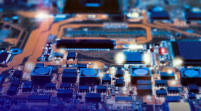
  Printed Circuit Boards (PCBs) are the fundamental building blocks of modern electronics, comprising a myriad of components meticulously arranged to enable the functionality of electronic devices. Identifying these components on a PCB and understanding their roles is essential for troubleshooting, repairs, and even designing electronic circuits.  In this comprehensive guide, we delve into the world of PCB components, unraveling their types, functionalities, and methods of identification.  Understanding PCB Components1. Resistors:  • Identification: Resistors are usually small, cylindrical components with colored bands indicating resistance values. Use a multimeter to measure resistance if the bands are unclear.  • Function: Resistors limit current flow in a circuit, adjusting voltage levels or protecting components.  2. Capacitors:  • Identification: Capacitors come in various shapes (cylindrical, rectangular) and sizes, often labeled with capacitance values and voltage ratings.  • Function: They store and release electrical energy, filtering signals or stabilizing voltage.  3. Diodes:  • Identification: Diodes appear as small cylindrical or square-shaped components with a stripe indicating polarity.  • Function: They allow current flow in one direction, blocking it in the opposite direction.  4. Transistors:  • Identification: Transistors come in different shapes (often three-legged), with part numbers indicating their type.  • Function: They amplify or switch electronic signals, serving as the basic building blocks of electronic devices.  5. Integrated Circuits (ICs):  • Identification: ICs are rectangular components with multiple pins. The part number often includes information about the manufacturer and type.  • Function: ICs integrate various functions (logic, memory, amplification) into a single package.  6. Inductors:  • Identification: Inductors resemble wire coils and are labeled with inductance values.  • Function: They store energy in a magnetic field and resist changes in current flow.  7. Connectors and Headers:  • Identification: Connectors are ports or slots for external connections. Headers are sets of pins for internal connections.  • Function: They facilitate the connection of external components or other PCBs.  Techniques for Identifying PCB componentsVisual Inspection:  Markings and Labels: Many components have printed markings indicating their values, part numbers, or manufacturers.  Physical Characteristics: Size, shape, and color often provide clues about a component’s type and function.  Multimeter and Testing:  Resistance Measurement: Use a multimeter in resistance mode to identify resistors and check for their values.  Capacitance Measurement: Multimeters with capacitance measuring capabilities can identify capacitors.  Datasheets and Component Manuals:  Online Resources: Manufacturers provide datasheets detailing component specifications and identification information.  Component Manuals: Some components have manuals with comprehensive details for identification.  Challenges and Conclusion  Identifying PCB components can present challenges due to the sheer diversity of shapes, sizes, and labeling conventions across manufacturers. Furthermore, miniaturization and surface-mount technology have made identification more intricate.  In conclusion, mastering the identification of PCB components is a foundational skill for electronics enthusiasts, engineers, and technicians. Utilizing a combination of visual inspection, testing tools, datasheets, and experience will empower individuals to decipher the complexities of PCBs, enabling effective troubleshooting, circuit design, and maintenance within the dynamic landscape of electronics.
2023-11-23 13:19 阅读量:1779
What is digital chip?  What is analog chip?
  In the field of chips, digital chips and analog chips are often compared together, and their differences are still very obvious. Let’s take a look at what the differences are between digital chips vs analog chips.  What is digital chip?      A digital integrated circuit, also known as a digital chip, is a digital logic circuit or system that integrates components and connections on the same semiconductor chip. Digital integrated circuits are designed and run based on digital logic (Boolean algebra) to process digital signals.  According to the number of gate circuits or components contained in digital integrated circuits, digital chips can be divided into small-scale integrated (SSI) circuits, medium-scale integrated MSI circuits, large-scale integrated (LSI) circuits, very large-scale integrated VLSI circuits and ultra-large-scale integrated circuits. integrated (ULSI) circuit.  According to the different characteristics of logic circuits, digital circuits can be divided into: sequential logic and combinational logic. If divided according to circuit structure, it can be divided into two series: TTL and MOS. There are many types of digital integrated circuits, including various gate circuits, flip-flops, counters, codecs, memories and hundreds of other devices.  Common digital chips include:  1. Data memory: such as EEPROM, FLASH memory, etc.  2. Microprocessors: such as x86, ARM, MIPS, etc.  3. Digital signal processor: such as DSP, image processor, etc.  4. Digital logic chips: such as TTL, CMOS, etc.  5. Digital signal converter: such as ADC, DAC, etc.  6. Digital signal controller: such as PWM, timer, etc.  What is analog chip?     Analog integrated circuits mainly refer to integrated circuits composed of capacitors, resistors, transistors, etc. that are integrated together to process analog signals. There are many analog integrated circuits, such as operational amplifiers, analog multipliers, phase-locked loops, power management chips, etc. The main circuits of analog integrated circuits are: amplifiers, filters, feedback circuits, reference source circuits, switched capacitor circuits, etc.  Analog chips mainly include power management chips and signal chain chips.  Among them, the power management chip is a chip that is responsible for the conversion, distribution, detection and other power management of electric energy in electronic equipment systems. The signal chain chip is a chip used in the path of signals from input to output in a system, including signal collection, amplification, transmission, processing and other functions.  Common analog chips include:  1. Amplifier chip: The amplifier chip is a common analog chip whose main function is to amplify the input signal.  2. Filter chip: The filter chip is an analog chip that can select the frequency of the input signal and can realize various filter functions such as low pass, high pass, and band pass.  3. Converter chip: The converter chip is an analog chip that can transform the input signal, and can realize the transformation of the frequency, phase, amplitude, etc. of the analog signal.  4. Power management chip: The power management chip is an analog chip that can manage input power and can realize various functions such as charging, discharging, and protecting of the power supply.  5. Sensor interface chip: The sensor interface chip is an analog chip that can process the sensor output signal and can achieve functions such as signal amplification, filtering, and transformation.  Digital chips vs analog chips – what are the differences  There are some key differences between digital and analog chips in terms of their basic units and internal circuitry. Digital chips usually adopt a CMOS structure and are composed of multiple identical unit circuits and one or more control circuits, which means that they are characterized by a high degree of repeatability. Different from this, analog chips are composed of various types of unit circuits, and there are relatively few repeated unit circuits.  In addition, the quiescent current characteristics of digital chips and analog chips are also different. Digital chips with CMOS structure have lower quiescent current, while the PN structure used in analog chips has higher quiescent current. However, analog chips often have a greater performance advantage in terms of dynamic range and are able to handle a wider range of signal amplitudes.  Digital chips and analog chips are each specifically designed to process digital and analog signals, and they cannot be used interchangeably. However, modern analog chips often contain digital circuitry to convert analog signals to digital signals for internal processing and then convert them back to analog signals for output. This hybrid design allows the full advantage of digital processing in the analog signal domain but still maintains the main characteristics of analog chips.
2023-11-16 11:08 阅读量:1744
  • 一周热料
  • 紧缺物料秒杀
型号 品牌 询价
RB751G-40T2R ROHM Semiconductor
CDZVT2R20B ROHM Semiconductor
BD71847AMWV-E2 ROHM Semiconductor
TL431ACLPR Texas Instruments
MC33074DR2G onsemi
型号 品牌 抢购
STM32F429IGT6 STMicroelectronics
BP3621 ROHM Semiconductor
ESR03EZPJ151 ROHM Semiconductor
TPS63050YFFR Texas Instruments
IPZ40N04S5L4R8ATMA1 Infineon Technologies
BU33JA2MNVX-CTL ROHM Semiconductor
热门标签
ROHM
Aavid
Averlogic
开发板
SUSUMU
NXP
PCB
传感器
半导体
相关百科
关于我们
AMEYA360微信服务号 AMEYA360微信服务号
AMEYA360商城(www.ameya360.com)上线于2011年,现 有超过3500家优质供应商,收录600万种产品型号数据,100 多万种元器件库存可供选购,产品覆盖MCU+存储器+电源芯 片+IGBT+MOS管+运放+射频蓝牙+传感器+电阻电容电感+ 连接器等多个领域,平台主营业务涵盖电子元器件现货销售、 BOM配单及提供产品配套资料等,为广大客户提供一站式购 销服务。

请输入下方图片中的验证码:

验证码