Embedded Die Packaging Emerges
Embedded die packaging is seeing renewed demand amid the push towards chips and systems that require smaller form factors.
ASE, AT&S, GE, Shinko, Taiyo Yuden, TDK, Würth Elektronik and others compete in the merchant embedded die packaging market, according to Yole Développement. In fact, ASE and TDK have a joint venture in the arena, which is beginning to ramp up production. Additionally, Texas Instruments and other IC makers develop their own embedded die packages.
Embedded die packaging is different than most package types. Generally, in many IC packages, the devices are situated on top of a substrate. The substrate serves as the bridge between the devices and a board in a system.
The term “embedded packaging” has different meanings. But in the world of embedded die packaging, the idea is to embed components inside the substrate using a multi-step manufacturing process. A die, multiple dies, MEMS or passives can be embedded in a side-by-side fashion in the core of an organic laminate substrate. The components are connected using copper-plated vias. All told, the embedded package resides on the board, which frees up space in a system.
Embedded die packaging isn’t new and has been relegated to niche applications due to various challenges, but the technology is promising. Using its proprietary embedded die technology, for example, TDK recently introduced the world’s smallest Bluetooth module. In addition, embedded die packaging provides many options, such as tiny packages, modules and system-in-boards (SiBs), for various applications.
“Clearly, the driver for embedding an active die in a substrate is size. You get a significant overall shrink in the ‘x’ and ‘y’ axis. That miniaturization allows you some design flexibility when you are looking at larger board layouts,” said Mark Gerber, director of engineering and technical marketing at Advanced Semiconductor Engineering (ASE). “When you look at the market today for embedded actives, it’s primarily centered around the power analog device area. Bluetooth WiFi modules are a key area because of the miniaturization aspects. Other applications include RF modules in the cell market.”
Embedded die packaging also has some drawbacks. There are some manufacturing challenges, as it combines the techniques used in advanced packaging and PCBs. Plus, the ecosystem is still relatively immature. “The cost of embedded die is still too high and the yield is sometimes too low,” said Vivienne Hsu, an analyst at Yole.
Still, the technology is making progress on several fronts, giving customers another option in the packaging landscape. In fact, the technology overlaps, and sometimes competes, against fan-out, leadframe packages and power modules, according to Hsu.
The embedded die packaging market is still a small business, as it is projected to grow from $15 million in 2017 to $18 million in 2018, according to Yole. By 2023, the market is expected to reach $50 million, according to Yole.
Packaging options
Embedded die is one of a plethora of IC packaging types. Basically, there are three broad categories in IC packaging—leadframe, wafer-level packaging (WLP) and substrate.
Used for analog and other markets, the leadframe group consists of several packaging types, such as quad-flat no-lead (QFN) and quad flat-pack (QFP). A leadframe is a metal frame. A die is attached to the frame and connected using thin wires.
WLP, the second category, involves two main package types—fan-in and fan-out. WLP involves packaging the die while it is still on the wafer. Generally, WLP is a substrate-less package. Instead of a substrate, WLP utilizes a thin-film of routing layers, or redistribution layers (RDLs), which provide electrical connections in the package.
The RDL layers are not connected to the board. Instead, WLP makes use of solder balls on the bottom of the package, which connects the RDLs to the board.
Meanwhile, substrate-based packages fall into several categories, such as ceramic and organic laminate. Ceramic substrates are based on aluminum oxide, aluminum nitride and other materials. Ceramic-based packages are used for surface-mount devices, CMOS image sensors and multi-chip modules.
Organic laminate substrates are used for 2.5D/3D, flip-chip and system-in-packages (SiPs). For these packages, the devices reside on top of the substrate. The materials used for organic substrates are FR-4 and others. FR-4 is composed of a woven fiberglass cloth with an epoxy resin.
These substrates use similar or identical materials as a printed-circuit board (PCB). So in some circles, organic substrates are sometimes referred to as a PCB.
Organic substrates are also multi-layer technologies, where at least two organic layers are separated by a metal layer. The metal layers act as an electromigration shield in the package.
Typically, IC packages reside on a board, which sometimes takes up valuable board space in a system. So why not embed the dies inside the substrate to save space and cost?
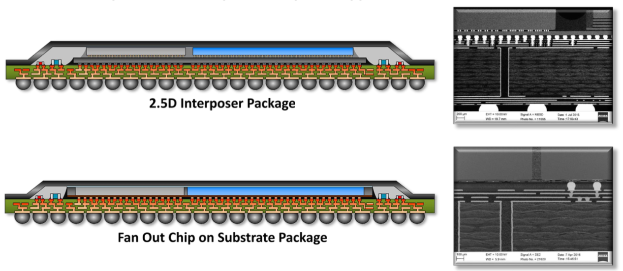
That’s where embedded die packaging comes in. This is not to be confused with fan-out. In fan-out, the dies are embedded in a reconstituted round wafer, based on a molded epoxy compound.
Embedded die packaging is different. The components are embedded inside a substrate, which has multiple layers. “The IC is embedded in the core of the substrate. This core is made of special resin. Besides the core resin, the other substrate layers are standard PCB material,” explained Nigel Lim, senior strategic marketing manager at TDK of America.
“The dies are typically placed side-by-side. TDK has experience with up to 2 to 3 dies placed side-by-side. For a standard 4-layer substrate, all of the dies are placed in-between layer 2 and layer 3. The dies are not stacked,” Lim said.
This provides several benefits. “The main benefits of the ECP technology in general are increased miniaturization, reliable interconnection, higher performance and improved protection of the integrated components,” according to Dietmar Drofenik, chief executive of the Advanced Packaging Business unit at AT&S, and Hannes Vorarberger, director of R&D at AT&S. AT&S, a supplier of PCBs and substrates, calls its embedded technology as Embedded Component Packaging (ECP).
“ECP in addition is supporting the trend towards modularization with lower set-up costs to other packaging technologies,” according to Drofenik and Vorarberger. “The hidden electronics (in embedded die) prevents against reverse engineering and counterfeiting.”
Embedded die is one of several ways to incorporate multiple dies into a package, but it isn’t the only option. “System-in-package is a big one. Fan-out also holds a lot of potential in this space due to cost. These packaging solutions bring better technical solutions to the market at lower prices,” said Cristina Chu, strategic business development director at TEL NEXX, part of TEL. [ASM Pacific has announced plans to acquire TEL NEXX from TEL.]
Another option is 2.5D/3D. All of these packaging types provide customers with different options. IC vendors can continue to develop system-on-a-chip (SoC) products using traditional chip scaling, but only a select few can afford the design costs at advanced nodes.
Another way to get the benefits of scaling is to put multiple devices in an advanced package, which may provide the functionality of an SoC at a lower cost. This is called heterogeneous integration.
Why embedded die?
For years the industry has embedded chips and passives in packages in one form or another, and embedded die packaging can be traced back to the 1990s, when GE and others introduced the technology. “TI’s MicroSIP was not the first, but one of the first volume products,” said Jan Vardaman, president of TechSearch International.
In fact, the technology began to take off in 2010 when Texas Instruments rolled out its MicroSiP power modules. With a 1mm thickness, the module embeds an IC in the substrate. In one configuration, TI embeds its PicoStar power management device in the substrate. Passives components are mounted on top of the package.
TI continues to sell MicroSiP. “We are embedding a specially designed and built PicoStar package (not the IC) inside the substrate/PCB. It’s the combination of the circuit IP, PicoStar, embedding, and passive integration that enables the value proposition. That is what allowed this technology to break through the barriers that constrained prior solutions,” said Sreenivasan Koduri, a TI fellow.
Others also expanded their efforts in the arena. In 2013, GE acquired Imbera, a pioneer in the market. And in 2015, ASE and TDK formed a joint venture in the arena.
By 2015, the embedded die packaging business reached $24 million, according to Yole. But in 2016 and 2017, the business declined due to a slowdown in a key market for the technology—camera modules for mobile devices, according to Yole.
Moreover, the product design cycles for embedded die took longer than expected. “Yield is one of the main challenges for embedded die,” TechSearch’s Vardaman said.
Today, though, embedded die packaging is seeing renewed growth. “It is growing gradually,” Yole’s Hsu said. “This technology is particularly interesting for better thermal management in industries such as the datacenter. Automotive is interested in this technology. It is mainly used for applications that require high power (better thermal management) or extreme miniaturization (less thickness).”
The technology still suffers from the same issues, namely cost, yield and others. “After embedding the die, it becomes hard to test the final product,” Hsu said. “The supply chain for embedded die is not mature yet.”
There are other issues. “In the PCB space, embedded passive film components (resistors, capacitors, inductors) are gaining traction in very small form-factor applications. The additional fabrication cost is somewhat offset by the reduced assembly cost,” said David Wiens, product marketing manager at Mentor, a Siemens Business. “Embedded actives are newer, and applicable to the same small form-factor situations. They are inherently more expensive, due to the lack of a rework process, and typically require some sort of a re-distribution layer.”
Recently, though, the industry has taken steps to bolster the technology. Several years ago, TDK introduced an embedded die technology called Semiconductor Embedded in Substrate (SESUB). TDK has produced several packages using SESUB, including the world’s smallest Bluetooth module.
SESUB is a proprietary solution, however. Generally, customers want a second source to ensure ample supply and better pricing.
Those were among the motives behind TDK’s move to form a venture with ASE in the arena. Prior to the joint venture, ASE participated in the market on two fronts. First, ASE has its own offering. Second, for customers who wanted SESUB, ASE would send the designs or components to TDK. TDK would build the packages for ASE.
Now, with the joint venture, ASE can provide the entire SESUB solution. ASE has put the equipment in place in a factory in Taiwan and is ramping up the technology.
In the basic SESUB flow, a wafer is processed in a fab. The wafer is thinned down to 50μm and the chips are diced up. Then the dies are placed on a separate panel, where they undergo a panel-level process. In panel, the idea is to process more dies than on a wafer in order to reduce the cost.
Panel-level processing is also being developed for other markets. The industry is developing fan-out packages on a panel-level format. This is different than panel-level embedded die packaging.
Meanwhile, in the embedded die flow, the dies are placed face up in the core of a substrate. The dies are placed side-by-side in one of the layers. “Then, you will end up laminating a material over the die. And then, you come back and laser down through that material to expose the pad. Then, you do a patterning process and plate up from there,” ASE’s Gerber said.
The end result is an embedded die package with a thickness from 260μm to 300μm. “In embedded die, there is not a limitation on how many die you can integrate. Most people try to keep it around four or less dies. The more die you embed, the higher risk for yield loss,” Gerber said.
The technology has some electrical and thermal benefits. “It’s is no different than if you are doing a 3D stacked solution like TSVs. You are bringing the dies closer together. The interconnections are shorter,” he said. “When you do the interconnect process on an embedded technology, you are building the routing layers up on top of the pads. So when I create a via or connection point down to a pad, I’m creating a solderless interconnect. It’s copper-to-copper. And from a reliability standpoint, there is not a whole lot to fail if your materials are matched properly.”
In SESUB, the most common configuration is an embedded package in a 4-layer substrate, but some are developing 2-, 5- and 6-layer options.
The technology is ideal for I/O counts up to 400. The line/space specs are 10μm and above. The pad pitch is 120μm with an 80μm pad size. “If you look into 2018 and 2019, that drops down to a 50μm pad pitch and a 30μm pad size,” he said.
Meanwhile, ASE offers its own embedded die technology, dubbed “Advanced Embedded Active System Integration (aEASI). In production for several years, aEASI is geared for high-power applications. It’s a hybrid package, which combines leadframe and substrate technology.
Other options
In 2008, a consortium was formed in Europe to commercialize embedded die packages. Austria’s AT&S commercialized the technology, called ECP.
“ECP uses the space in an organic laminate substrate to embed actives (chips) and/or passive components,” according to AT&S’ Drofenik and Vorarberger. “Capacitors and resistors are available as thin components with copper terminations, while varistors and thermistors are under development.”
MEMS can also be integrated into a package. Like SESUB, ECP is processed using a panel-level format. “The embedded process can be broken down into three main steps: component assembly (core structuring, cavity cutting, tape lamination); lamination (resin fill, tape removal); and structuring (laser drilling, e-test),” according to Drofenik and Vorarberger.
The technology can be used in automotive, communications, medical, mobile and other apps. “Typical applications where the technology is already used today are portable electronics like wearables, MEMS, modules for wireless connections, medical products like hearing aids, identification systems or the fan-out- implementation for fine-pitch ICs,” they said.
What next? The technology is moving towards what AT&S calls “all-in-one” modules. It’s an evolution of today’s technology. It involves the development of more integrated and smaller modules using advanced PCB-like substrates and packaging.
For this, customers will have a range of new component and technology options for the package. This includes insulated metallic substrates, multi-layer substrates, HDI, flexible PCBs and interposers. “New high-end systems, such as advanced SIPs and SiBs (system-in-boards) can be largely combined in modular form with all basic technologies,” according to Drofenik and Vorarberger.
Embedded die packaging is promising. If it can overcome some challenges, it may take off. If not, it might remain a niche technology. Worse, it could get lost in the shuffle in the confusing packaging landscape.
在线留言询价
New Issues In Advanced Packaging
- 一周热料
- 紧缺物料秒杀
| 型号 | 品牌 | 询价 |
|---|---|---|
| TL431ACLPR | Texas Instruments | |
| CDZVT2R20B | ROHM Semiconductor | |
| RB751G-40T2R | ROHM Semiconductor | |
| MC33074DR2G | onsemi | |
| BD71847AMWV-E2 | ROHM Semiconductor |
| 型号 | 品牌 | 抢购 |
|---|---|---|
| BP3621 | ROHM Semiconductor | |
| TPS63050YFFR | Texas Instruments | |
| BU33JA2MNVX-CTL | ROHM Semiconductor | |
| IPZ40N04S5L4R8ATMA1 | Infineon Technologies | |
| ESR03EZPJ151 | ROHM Semiconductor | |
| STM32F429IGT6 | STMicroelectronics |
- 周排行榜
- 月排行榜
AMEYA360公众号二维码
识别二维码,即可关注


请输入下方图片中的验证码:


