Fab Equipment Challenges For 2019
After a period of record growth, the semiconductor equipment industry is facing a slowdown in 2019, in addition to several technical challenges that still need to be resolved.
Generally, the equipment industry saw enormous demand in 2017, and the momentum extended into the first part of 2018. But then the memory market began deteriorating in the middle of this year, causing both DRAMand NAND vendors to push out their equipment orders.
The memory downturn is expected to extend into 2019, which will impact equipment makers with exposure to DRAM and NAND. Then, on the geopolitical front, the trade issues between the United States and China are a cause for concern, although the long-term impact remains unclear.
On the positive side, foundry vendors continue to ramp up their 7nm processes, propelling equipment orders in the logic space. The outlook is good at the other end of the spectrum, as well, where the industry continues to see demand for mature 200mm equipment.
Still, the demand for leading-edge and mature tools can’t make up for the downturn in memory, which likely will put the equipment industry in negative territory. In total, the worldwide semiconductor equipment industry is expected to grow by 13.7% in 2018, but the business is projected to slow and decline by 8.6% in 2019, according to VLSI Research.
Of course, the forecast could change overnight, and it’s not all gloomy in the market. Tool segments with exposure to logic will fare better in 2019. But amid a downturn in memory, tool segments with exposure to DRAM and NAND are in for a rough ride.
For example, some foundries are expected to ramp up extreme ultraviolet (EUV) lithography at 7nm, a move that will likely propel EUV scanner orders for ASML. Inspection and metrology are also bright spots.
“If you look at the equipment side, EUV is obviously going to be positive. The other one that you see performing better in downturns is process control. If foundry and logic maintain their spending, they are heavy on process control compared to memory,” said Risto Puhakka, president of VLSI Research. “On the negative side, you will probably see etch and some deposition segments that are heavily dependent on memory. That will probably see a bigger decline.”
To help the industry get ahead of the curve in 2019, Semiconductor Engineering has taken a look at several equipment segments, including foundry, memory, China and 200mm.
More numbers
What a difference a year makes. Citing huge demand for memory, the semiconductor market is projected to grow by 15.5% in 2018, according to VLSI Research. But the current memory slowdown is expected to drag down the industry, causing the IC market to decline by 1.6% in 2019, according to the firm.
The equipment industry is following a similar pattern. 2018 started out looking like another record year for the equipment industry, but the memory downturn slowed the momentum.
“The equipment market will grow about 14% in 2018, which is a little bit below what we were predicting earlier in the year. But still, it’s a good year,” said Andrea Lati, an analyst with VLSI Research. “But we did see a de-acceleration in the second half of 2018, which we expected. If you look how much spending went on in 2017, we knew at some point that supply was going to catch up with demand and surpass it. That happened in the second half of this year.”
At that point, the market failed to regain the momentum. “This downward pressure we are seeing in the second half of 2018 is going to roll over into 2019. We’re a little bit more bearish about 2019. We do expect both the semiconductor and the equipment markets to decline in 2019,” Lati said. “Part of it is because there is some over-build in our industry. The second part is really the macro picture. It’s slowing, and we also have the China situation. That is also adding uncertainty.”
Compounding the problem is the memory downturn. “We expect memory sales to decline almost 10% in 2019. We do see that logic will probably be in positive territory and growing almost 4%. So it will be primarily a memory-driven downturn in 2019,” Lati said.
Needless to say, this will impact the equipment industry. In a different forecast, SEMI predicts that worldwide sales of new semiconductor equipment will increase 9.7% to $62.1 billion in 2018, but the market will decline by 4% in 2019. In 2019, South Korea will remain the largest equipment market, followed by China and Taiwan, according to SEMI.
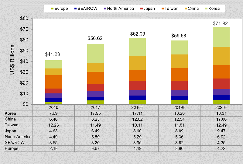
Fig. 1: Worldwide sales of new semiconductor manufacturing equipment. Source: SEMI
Two other metrics, semiconductor capital spending and the wafer-fab equipment (WFE) market, are seeing similar trends.
“(For) WFE CapEx, calendar 2018 was driven by buoyant demand for memory,” said Toshiki Kawai, president and chief executive of TEL, in a recent presentation. “Expect year-over-year growth of approximately 5%-10%.”
In 2019, though, WFE will reach $50.6 billion, down 5% over 2018, according to KeyBanc Capital Markets. Capital spending will reach $87.2 billion in 2019, down 5% over 2018, according to KeyBanc.
“For memory, what we are seeing right now is a definite slowdown. I see a CapEx decrease in ’19 for DRAM after an incredible year. In NAND, it will be modestly down in ’19,” said Oreste Donzella, senior vice president and chief marketing officer at KLA-Tencor. “We believe foundry will go up. The question is how much will foundry go up.”
From an applications perspective, it’s also a mixed picture. The smartphone market is flat, but there are other applications that will drive IC demand, such as automotive, artificial intelligence and wireless.
AI involves a technology called machine learning. In simple terms, machine learning uses a neural network in a system. In neural networks, a system crunches data and identifies patterns. It matches certain patterns and learns which of those attributes are important.
The industry is accelerating the use of machine learning in various systems, thereby driving the demand for ASICs, FPGAs, GPUs and memory.
“The world of memory is increasing in the era of AI and deep learning,” said Gill Lee, managing director of memory technology at Applied Materials. “Bit growth is happening with all of these new applications, such as AI, deep learning and data centers. The memory applications are becoming more diversified.”
Others see similar trends. “Startup funding for semiconductor companies is back up, with similar increases for new programs inside existing companies,” said Aki Fujimura, chief executive of D2S.
“Excitement over deep learning, autonomous driving, and continued innovation in IoT are providing new design starts,” Fujimura said. “Despite the recent hiccup from the cooling off in cryptocurrency, I continue to see a strong rising tide behind Nvidia for simulation of natural effects, image and video processing, and deep learning. It is great to see a new wave of funding of innovation in new chips, particularly driven by deep learning. We are going to see deep learning improve what we do in semiconductor manufacturing, as well, in 2019.”
Thirumal Thanigaivelan, senior marketing director at Veeco’s UItratech division, said: “Diverse market requirements in AI, graphics and automotive are driving leading-edge development. We expect the investment to continue as we drive toward more processing capability in HBM (high-bandwidth memory). The diverse markets and applications space dampens the fluctuations in fab equipment spending, reducing the cyclicality.”
Wafers and masks
One way to get a pulse on the market is to look at the demand picture for two key building blocks in the IC sector—silicon wafers and photomasks.
In 2019, silicon wafer shipments will reach 13,090 million square inches, up 5.2% over 2018, according to SEMI. In 2018, silicon wafer shipments grew 7.1%.
Then, the photomask market is forecast to exceed $4 billion in 2019, up 4% over 2018, according to SEMI.
Photomask makers see demand for both leading- and trailing-edge masks. For example, EUV mask shipments are expected to double, from 1,041 in 2017 to 2,185 in 2018, according to a survey from the eBeam Initiative. That’s a small percentage of overall mask shipments, as 587,233 photomasks will be delivered in 2018, up 27% over 2017, according to the survey.
“EUV masks went up 2X, which is expected. That’s a good thing. But the numbers are insignificant compared to the overall masks that are reported. But taken by itself, a 2X increase is a strong indication that the industry is getting ready for EUV,” D2S’ Fujimura said.
EUV lithography—a next-generation technology that patterns tiny features on a chip—is moving into high-volume production in 2019 after years of delays. In an EUV scanner, a power source converts plasma into light at 13.5nm wavelengths, enabling the system to print fine features.
Chipmakers need EUV because it’s becoming more difficult to pattern the tiny features using today’s 193nm immersion lithography and multiple patterning.
Foundry growth
Meanwhile, the foundry business, which is a big equipment market, is a mixed bag. Capital spending in the foundry sector will reach $25.1 billion in 2019, up 14% over 2018, according to KeyBanc.
But the number of leading-edge foundries is dwindling, meaning there are fewer buyers of equipment at the most advanced nodes.
Tool vendors are seeing demand in several foundry segments. At the high end, the demand driver is 7nm, although the product mix is changing at advanced nodes. “20nm, 16nm, 14nm and 10nm were really driven by mobile,” KLA-Tencor’s Donzella said. “At 7nm, we still have a high number of tape-outs driven by mobile. We also see AI applications. Now, the question is how many of these tape-outs are going to be realized in wafer capacity.”
Not all of the action is at advanced nodes. “If you look at the percentage of revenue coming from the trailing edge, say 40nm and above, it’s still quite significant. Some 50% of the foundry revenue comes from trailing edge. That isn’t going to change. The reason is because of IoT demand, driving RF and MEMS. Then, you have automotive,” Donzella said.
At 22nm and above, the industry continues to develop chips based on traditional planar transistors. In contrast, 16nm/14nm and 10nm/7nm are based on finFETs.
It’s becoming more difficult to scale at each node. “PPAC (power, performance, area, cost) scaling at the leading edge is getting more complex and costly,” said Yang Pan, corporate vice president of advanced technology development at Lam Research.
The challenges have caused a major shakeup in the leading-edge foundry landscape. Today, there are only two companies shipping 7nm—Samsungand TSMC. In 2018, GlobalFoundries halted its 7nm efforts. The company couldn’t justify the return-on-investment at 7nm, as only a few customers can afford to design chips at advanced nodes. At the same time, Intel is struggling at 10nm and has delayed it several times. (Intel’s 10nm is roughly equivalent to 7nm from the foundries.)
Still, Samsung and TSMC are moving ahead at 7nm, but they will face challenges along the way. In 2018, TSMC moved into production at 7nm using traditional optical lithography. Then, TSMC plans to insert EUV for its second version of 7nm, which is slated for early 2019.
Samsung recently announced 7nm using EUV. Then, at some point, Intel is expected to insert EUV.
Bringing up EUV into production presents some challenges. “The introduction of EUV creates new challenges and opportunities for new patterning films and advanced etch processes such as atomic layer etching. Multiple patterning, complementary to EUV, will continue to drive density scaling,” Lam’s Pan said.
There are other challenges at advanced nodes. “The other grand challenge in PPAC scaling is RC (resistive-capacitance) reduction, which requires new materials and integration to reduce line and via resistance to improve circuit power performance,” Pan said.
Memory woes
Memory, another big market for equipment, is in a difficult period. In early 2018, the NAND market declined and fell into an oversupply mode. Oversupply has extended throughout 2018, while prices have plummeted.
The NAND outlook is gloomy. “For NAND flash, 2019 revenues should be down 40% from 2018,” said Jim Handy, an analyst at Objective Analysis. “I expect for NAND to reach cost and hug the cost curve until the current oversupply situation ends in a couple of years.”
The DRAM market faces a similar situation after years of growth. “DRAM is just beginning a collapse that NAND has been undergoing since early this year,” Handy said.
And if that isn’t enough, there are some technical challenges in memory. For example, planar NAND has reached its physical limit at the 1xnm node. So, NAND vendors have been migrating from planar NAND to 3D NAND. Both types are used for solid-state storage drives (SSDs).
Unlike planar NAND, which is a 2D structure, 3D NAND resembles a vertical skyscraper in which horizontal layers are stacked and then connected using tiny vertical channels.
Today, vendors are migrating from 48- to 96-layer 3D NAND devices with 128-layer products in R&D. Some refer to layers as pairs.
The bit density increases as you add more layers. “In 2018, we’ve seen 96 pairs come into the market. Next year, I expect that we will see the next-generation technology, something larger than 120,” Applied’s Lee said.
Continued scaling of 3D NAND will drive down the bit cost, enabling high-density SSDs at lower prices. This in turn expands the market for SSDs. “NAND-based SSDs were originally targeted for more of the high end. Now, it’s a big part of notebook computers. SSDs are also targeting even the low-end of storage. So, the market for NAND is not only going up, but it’s also covering a big part of the hard disk-drive market,” Lee said.
Still, it’s difficult to scale 3D NAND from 64 to 96 layers and beyond. In the 3D NAND flow, alternating films are stacked on a substrate using deposition. The process is repeated several times. But as more layers are added, the challenge is to stack the layers uniformly and without defects.
In the next step, a plasma etcher etches tiny circular holes or channels from the top of the device stack to the bottom substrate. Each channel must be uniform. Otherwise, CD variations may occur.
“Stress management is another area of extreme importance when the layer count increases,” Lam’s Pan said. “High aspect ratio (HAR) etch continues to be the most critical and difficult step in the entire flow. At 96 layers and above, not only does the memory hole module get more challenging, other structures such as slits also become critically difficult with layer stacking.”
China and 200mm
For years, China has been a growing market for semiconductor equipment. Trade issues, however, are infusing uncertainty in this arena.
In China there are two types of chipmakers—multinational and domestic players. “The domestic semiconductor companies have been spending quite a bit. And the business is up at all major equipment suppliers in 2018,” VLSI Research’s Puhakka said.
What about 2019? ‘’I don’t expect overall WFE from China to change significantly between ’18 and ’19,” KLA-Tencor’s Donzella said. “The mix is different. We see more foundry and less memory. We see more foreign investment and less local.”
Meanwhile, 200mm is also a key equipment market. Demand for analog, MEMS and RF chips continue to cause shortages for 200mm fab capacity and equipment.
“Some of the Asian foundries are afraid of lower orders in the second half of 2018. However, the current utilization of most fabs in Asia is over 90%,” said Bruce Kim, chief executive of SurplusGlobal, a supplier of secondary equipment. “There is still a big demand for 200mm tools.”
What about 2019? “It will be very tight. Some of the advanced devices will be moved from 200mm to 300mm. I estimate the 300mm transfer won’t be so large in 2019,” Kim said.
Heading into 2019, there is a shortfall of 200mm equipment. The industry requires from 2,000-3,000 new or refurbished 200mm tools to meet fab demand, according to SurplusGlobal. But there are only 500 available 200mm tools on the market, according to the company.
200mm tool prices will remain high. “300mm tool prices are lower than 200mm tool prices these days,” Kim said.
All told, 2019 looks cloudy for the equipment industry. Foundry looks up, but memory is down. And so, equipment vendors will need to hold on tight. It will likely will be a stormy ride over the next year.
在线留言询价
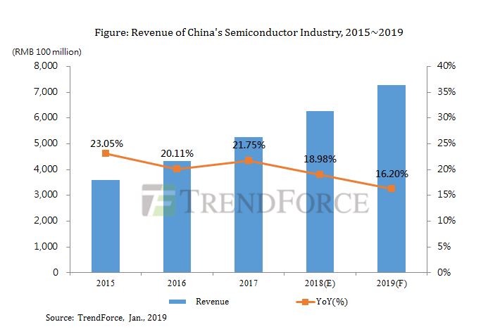
Revenue Growth in China's Semiconductor Industry Would Slow Down to 16.2% in 2019 due to Pessimistic
- 一周热料
- 紧缺物料秒杀
| 型号 | 品牌 | 询价 |
|---|---|---|
| CDZVT2R20B | ROHM Semiconductor | |
| RB751G-40T2R | ROHM Semiconductor | |
| TL431ACLPR | Texas Instruments | |
| BD71847AMWV-E2 | ROHM Semiconductor | |
| MC33074DR2G | onsemi |
| 型号 | 品牌 | 抢购 |
|---|---|---|
| ESR03EZPJ151 | ROHM Semiconductor | |
| BP3621 | ROHM Semiconductor | |
| BU33JA2MNVX-CTL | ROHM Semiconductor | |
| TPS63050YFFR | Texas Instruments | |
| STM32F429IGT6 | STMicroelectronics | |
| IPZ40N04S5L4R8ATMA1 | Infineon Technologies |
- 周排行榜
- 月排行榜
AMEYA360公众号二维码
识别二维码,即可关注


请输入下方图片中的验证码:
