Distributed Architecture Puts the ‘Reality’ in AR
For the last 40 years, the evolutionary path for chipsets for mobile electronics has inexorably been headed toward increasing levels of functional integration, culminating in the system-on-chip (SoC) architecture.
Sometimes monolithically integrated and at other times achieved through advanced packaging, mobile SoCs incorporate multiple functions — including, but not limited to, the baseband, applications processor, RF transceiver, WLAN (i.e., Wi-Fi) and WPAN (i.e., Bluetooth) communications — into a single chip or package. Such an architecture is ideal for the thin but powerful form factors that ultimately embody modern cellphones. However, as we go beyond the smartphone to a whole new augmented-reality (AR) world — some call this the metaverse — through the portal of AR glasses, the SoC architecture is proving to be more of a hindrance than an enabler.

To turn the vision (pun intended) of AR glasses into reality, designs need to not only achieve mass-market adoption but must also be able to be worn on an everyday basis — as part of the wearer’s daily attire. In order to achieve this, glasses are required to be more streamlined than smartphones. They also need to enable fashionable form factors. Additionally, to minimize wearer fatigue, they not only have to be as light as possible but also be more balanced in terms of weight distribution to keep from having one side of the glasses be heavier than the other.
Past and current designs have typically located the electronics in the temple, or arms, of the glasses, and this continues to be a logical place. However, mobile SoCs do not lend themselves to addressing the challenges above, given their die and package size and the fact that being a single chip does not allow for any sort of weight distribution other than potentially adding more bulky components like batteries on the other arm.
At this year’s Snapdragon Summit, Qualcomm announced a departure from the SoC evolutionary path that could potentially bring AR glasses to reality. Reversing the trend, Qualcomm proposed a distributed architecture approach not only for the electronics inside the glasses but also between the glasses and a host device like a smartphone or PC distributing some of the heavy lifting for both cellular communications and some of the graphics processing.
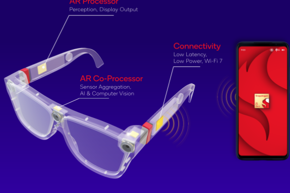
On the second day of the Snapdragon Summit, Qualcomm announced the new Snapdragon AR2 Gen 1 platform. The platform breaks up the various silicon blocks into three modules that are spaced around the glasses, which enables designs that are more streamlined and balanced. The modules include an AR processor, an AR co-processor and a Wi-Fi connectivity module.
As announced, the AR processor will be responsible for typical GPU-type functions like image/video capture, computer vision and display driving but doing so in a hardware-accelerated fashion by incorporating ISP, Adreno Video, Adreno Display and visual analytics engine IP blocks.
Meanwhile, the AR co-processor will be focused on providing AI acceleration, as well as aggregating sensor and camera data for tasks like eye tracking, object detection and biometric authentication.
Last but not least, the connectivity module will of course be responsible for the high-speed, low-latency communications needed to make the distributed architecture viable. What might not be as obvious is the module’s use of Qualcomm’s FastConnect XR 2.0 software suite, which the company is touting as enabling a 40% reduction in power compared with previous versions while delivering the required performance.
在线留言询价
- 一周热料
- 紧缺物料秒杀
| 型号 | 品牌 | 询价 |
|---|---|---|
| TL431ACLPR | Texas Instruments | |
| RB751G-40T2R | ROHM Semiconductor | |
| BD71847AMWV-E2 | ROHM Semiconductor | |
| MC33074DR2G | onsemi | |
| CDZVT2R20B | ROHM Semiconductor |
| 型号 | 品牌 | 抢购 |
|---|---|---|
| BU33JA2MNVX-CTL | ROHM Semiconductor | |
| TPS63050YFFR | Texas Instruments | |
| IPZ40N04S5L4R8ATMA1 | Infineon Technologies | |
| BP3621 | ROHM Semiconductor | |
| ESR03EZPJ151 | ROHM Semiconductor | |
| STM32F429IGT6 | STMicroelectronics |
- 周排行榜
- 月排行榜
AMEYA360公众号二维码
识别二维码,即可关注


请输入下方图片中的验证码:


