TSMC’s U.S. Factory Plans Small-Scale Trial Line for Q1 2024

发布时间:2023-09-08 17:00
作者:AMEYA360
来源:网络
阅读量:2917

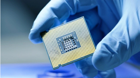
  According to a report by Taiwan’s Money DJ, the production schedule for TSMC’s semiconductor foundry in the United States has been delayed until 2025, raising concerns among observers. However, Chairman Mark Liu, in an interview on the 6th, stated that there has been significant progress over the past five months and expressed confidence in the project’s success. Industry sources have indicated that TSMC’s U.S. facility may alter its ramp-up strategy by first establishing a mini-line for trial production, with the expectation of having it in place by the first quarter of 2024.

TSMC’s U.S. Factory Plans Small-Scale Trial Line for Q1 2024

  TSMC’s Fab 21 Phase 1 construction began in April 2021, originally slated for early 2024 production. However, challenges such as a shortage of skilled equipment installation personnel, local union protests, and differences in overseas safety regulations have caused delays in equipment installation. This has compelled TSMC to adjust its plans, and the expected production timeline is now set for 2025, representing a one-year delay.

  Industry analysts have noted that the efficiency of equipment entering the facility at TSMC’s U.S. plant in Arizona is only about one-third of that of its Taiwan facilities. Given the current pace of progress, the time required for equipment setup to actual production could be substantial. Therefore, TSMC has decided to change its previous ramp-up strategy and first establish a mini-line with an initial estimated monthly capacity of about 4,000 to 5,000 wafers. This approach aims to ensure some level of production output while mitigating potential contract breach issues arising from delays in production.

(备注:文章来源于网络,信息仅供参考,不代表本网站观点,如有侵权请联系删除!)

在线留言询价

相关阅读
Unlocking Compound Semiconductors’ Economy-driving Potential
  Silicon-based semiconductors and advances in computing technology have transformed our world within a short time frame. Nevertheless, we have now reached the limit of where silicon alone can take us, and innovative approaches are required for enabling the necessary advances in our digital lives.  Our collective experience with the Covid-19 pandemic has demonstrated beyond a doubt that being connected is no longer optional. Fully realizing our individual roles in this emergent, interconnected society requires us to participate via our smart devices over increasingly powerful and intertwined networks.  New technologies ranging from the internet of things, Industry 4.0, and 5G/6G to electric/autonomous vehicles and augmented reality are placing unprecedented demands on incumbent semiconductors. Rising performance requirements leave traditional silicon semiconductors unable to address the challenges.  What, then, is the solution?  A way forward is available at the level of the semiconductor materials themselves: We must look beyond silicon. And there is a group of complementary semiconductor materials that can provide the opportunity to reach where silicon cannot.  Compound semiconductors, meaning those formed from two or more elements, include materials such as gallium nitride, gallium arsenide, and indium phosphide. These semiconductors are already powering many of the technologies on which our interconnected world relies. At the same time, their adoption is rapidly accelerating (growing at double the rate of silicon), and they are becoming mainstream in power electronics, sensing, connectivity, and advanced display applications.  But the growth story does not stop there. To achieve the next wave of innovation, engineers are marrying compound semiconductors with silicon to deliver a new generation of products that will be highly disruptive in terms of the performance attributes they offer, and at a scale that will enable the mass adoption of compound semiconductors.  The growth of compound semiconductors is enabled by epitaxy, the fundamental production process used to architect atomically engineered structures from which chip companies build electronic and optoelectronic devices. By selecting the right compounds and precisely controlling how the materials are deposited on a substrate, epitaxial-wafer producers have at their disposal a unique materials “toolset” that lets them tailor wafers to enable a wide variety of device types, from power amplifiers to sensors to lasers. The level of customization that epitaxy enables is unrivaled; hence, it is the key building block of the compound-semiconductor ecosystem.  The silicon industry and its foundries have built their success upon increasingly advanced lithography techniques, mastering successive process node generations and thereby producing progressively smaller transistor technologies — 5 nm, 2 nm, and so on.  Epitaxy is to compound semiconductors what lithography is to silicon. Epitaxy thus will be central to our efforts to move beyond traditional feature scaling based on Moore’s Law.  But how does one go about turning the potential of compound semiconductors into reality — and educating an industry that is accustomed to decades of reliance on silicon-based solutions? Simply put, we need open-access foundries to start producing state-of-the-art compound semiconductors.  By way of analogy, compare Intel with TSMC in the silicon space. How many designs per month does Intel work on? One or two? Half a dozen? Now consider TSMC, which is constantly adapting its processes to various designs, forcing it to learn, adapt, and improve continuously. These “best practices” benefit everyone in the chain, from the foundry all the way to the end user.  The same situation manifests itself in the compound-semiconductor segment. Some vertically integrated chipmakers are convinced that it is optimal to produce their epitaxy in-house. However, they can never learn as fast or be as agile as an open-access foundry that is constantly collaborating with multiple customers on multiple designs. This process of building experience and knowledge gives the open-access foundry model a significant edge in the innovation race.  Further, the environmental aspects of chip manufacture can no longer be ignored. The semiconductor industry must be “carbon responsible” and minimize the lifetime impact of its materials and processes. Resources can no longer be viewed as infinite. Energy consumption has consequences. The semiconductor industry must find a way to build a digital, interconnected world that is compatible with the global push toward zero net emissions. Advanced compound-semiconductor materials are enabling the industry to innovate, and thanks to their well-documented performance and efficiency attributes versus silicon, compound semiconductors provide a key building block along the path to net zero.  I was speaking recently with several key figures from the silicon industry who echoed these trends. They increasingly recognize the importance of compound semiconductors and acknowledge the strategic importance of epitaxy. In particular, there is a recognition of the enablement that compound semiconductors provide to the silicon industry.  As a result, the silicon- and compound-semiconductor advancements are no longer separate pursuits; rather, the two industries are more significantly collaborating to deliver disruptive technologies at scale. Epitaxy plays a critical role in this work.  Semiconductors are vital to the world economy. And with an ever-increasing focus on energy efficiency and ubiquitous connectivity, compound semiconductors are poised to deliver the next-generation technology solutions that silicon simply cannot.
2023-01-10 11:02 阅读量:2938
  • 一周热料
  • 紧缺物料秒杀
型号 品牌 询价
CDZVT2R20B ROHM Semiconductor
BD71847AMWV-E2 ROHM Semiconductor
MC33074DR2G onsemi
RB751G-40T2R ROHM Semiconductor
TL431ACLPR Texas Instruments
型号 品牌 抢购
ESR03EZPJ151 ROHM Semiconductor
TPS63050YFFR Texas Instruments
BP3621 ROHM Semiconductor
IPZ40N04S5L4R8ATMA1 Infineon Technologies
BU33JA2MNVX-CTL ROHM Semiconductor
STM32F429IGT6 STMicroelectronics
热门标签
ROHM
Aavid
Averlogic
开发板
SUSUMU
NXP
PCB
传感器
半导体
相关百科
关于我们
AMEYA360微信服务号 AMEYA360微信服务号
AMEYA360商城(www.ameya360.com)上线于2011年,现 有超过3500家优质供应商,收录600万种产品型号数据,100 多万种元器件库存可供选购,产品覆盖MCU+存储器+电源芯 片+IGBT+MOS管+运放+射频蓝牙+传感器+电阻电容电感+ 连接器等多个领域,平台主营业务涵盖电子元器件现货销售、 BOM配单及提供产品配套资料等,为广大客户提供一站式购 销服务。