SK hynix Reportedly Builds Silicon Valley HBM Team to Boost Customer Co-Design With U.S. Big Tech
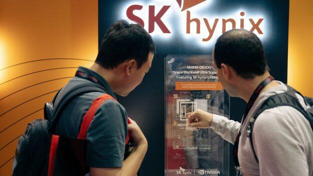
  SK hynix is reportedly strengthening its HBM co-design capabilities in Silicon Valley as it deepens collaboration with global Big Tech customers. According to NewsPim, sources say SK hynix America operates an HBM Architect Design Team in San Jose, California, working directly with major U.S. customers on base-die design for HBM and 3D-stacked DRAM. The team develops next-generation HBM architectures around customer requirements, going beyond local technical support to collaborate throughout product development.  Notably, NewsPim adds that SK hynix is expanding the team, offering annual salaries of US$150,000–US$260,000. The company is seeking experience in DRAM and HBM architecture, full-custom and digital co-design, power delivery network (PDN) analysis, and logic foundry design, with experience in 1x-nanometer DRAM and foundry nodes of 3nm or below preferred. Developing advanced, customer-tailored HBM architectures for future products is among the team’s core responsibilities, the report notes.  The San Jose location also supports this strategy. As NewsPim notes, NVIDIA and AMD are headquartered in nearby Santa Clara, while Broadcom has operations in San Jose. Positioning HBM engineers near these major AI chip design hubs allows SK hynix to work directly with customers on next-generation products and quickly relay their requirements to development teams in South Korea.  SK hynix is already deepening such collaboration with NVIDIA. Chosun Ilbo notes that the two companies are jointly developing next-generation memory for AI factories, expanding their partnership beyond supplying existing HBM toward developing advanced memory aligned with NVIDIA’s next-generation roadmap.  Customer Co-Design Reshapes HBM Competition  Customer co-design is expected to become even more important with HBM4 and future generations. As NewsPim notes, increasingly diverse AI accelerator architectures are driving different requirements for HBM capacity, bandwidth, and power, making early co-optimization of AI chips and memory increasingly important.  This is also reshaping HBM competition. Memory suppliers that participate early in customers’ next-generation AI chip development can incorporate specific requirements into their designs, while co-developed HBM may raise barriers for rivals seeking to enter the same supply chain later. As the report points out, such collaboration is becoming increasingly important for securing next-generation HBM orders.  The trend extends beyond SK hynix. Seoul Economic Daily notes that Samsung is recruiting base-die designers as customer-specific optimization for AI accelerator vendors becomes increasingly important with HBM4. The company is also hiring application engineers to evaluate HBM on AI accelerator systems and support key customer qualifications, with the aim of shortening the certification process.
Key word:
Release time:2026-08-20 11:44 reading:204 Continue reading>>
TSMC Arizona Profit Soars 663% YoY in 1H26; U.S. Earnings Pull Back 8.2% QoQ in 2Q as Depreciation Bites
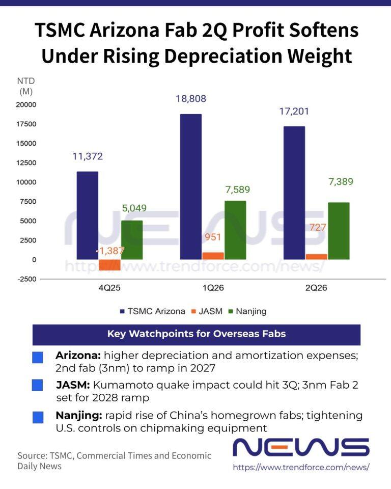
  As TSMC’s Arizona fabs ramp up to meet strong demand from NVIDIA and other Big Tech customers, the U.S. unit has overtaken TSMC Nanjing as the foundry giant’s most profitable overseas subsidiary. Citing TSMC’s 1H26 interim report, Commercial Times and the Economic Daily News report that TSMC Arizona posted a record NT$36.066 billion profit in 1H26, up 662.8% YoY.  As TSMC’s overseas footprint moves into a profit-harvesting phase, its four major manufacturing subsidiaries generated a combined NT$58.529 billion in 1H26, up 215.4% YoY. TSMC Arizona alone contributed more than 60% of the total, underscoring its growing weight in TSMC’s overseas earnings mix, as highlighted by the Economic Daily News.  Arizona Fab Profit Pulls Back QoQ as Depreciation Pressure Mounts  However, the Arizona profit surge showed signs of moderating in Q2. Its profit slipped 8.2% QoQ to NT$17.259 billion, even as it remained up a hefty 307.8% YoY, according to the Economic Daily News. Commercial Times further notes that TSMC recognized about NT$14.603 billion in investment income from its U.S. fab in the second quarter, down 13.6% from NT$16.909 billion in the first quarter.  Analysts cited by Commercial Times pointed out that as construction of subsequent fabs accelerates, higher depreciation and amortization expenses could put pressure on profitability.  TSMC has already warned that the overseas fab ramp-up will weigh on margins. CFO Wendell Huang said at the July earnings call that overseas expansion is expected to dilute gross margin by 2–3 percentage points in the early stages, widening to 3–4 points as the fabs mature.  As highlighted by Commercial Times, TSMC’s first Arizona fab entered 4nm mass production in 4Q24, while the second, focused on 3nm, is slated to ramp in 2H27. With the latest $100 billion investment, total planned U.S. investment has reached $265 billion, with the Arizona site ultimately expected to house 10 fabs and two advanced packaging facilities, according to MoneyDJ. How this aggressive expansion will impact profitability remains a key watchpoint.  Nanjing, JASM Profits Ease as Overseas Earnings Face New Tests  TSMC’s Nanjing fab remained a key profit driver, posting NT$14.978 billion in 1H26 and ranking second among its four major overseas operations. However, Q2 profit edged down to NT$7.389 billion from NT$7.589 billion in Q1, according to Economic Daily.  Meanwhile, JASM’s earnings also cooled slightly in Q2. As noted by Commercial Times, the Japan subsidiary, 73%-owned by TSMC, turned profitable this year after posting a loss in 2025, earning NT$951 million in Q1 and NT$727 million in Q2.  The bigger question now is whether JASM can keep that momentum after the July 7.1-magnitude Kumamoto earthquake. Commercial Times notes. The fab has resumed normal production and passed structural safety checks, but equipment requalification, calibration and wafer losses could reportedly weigh on Q3 results.
Key word:
Release time:2026-08-18 11:25 reading:205 Continue reading>>
TSMC and Researchers Overcome 2D Semiconductor Bottleneck with Epitaxial Interface Engineering
  As conventional silicon semiconductor technology approaches its physical limits, 2D semiconductors are increasingly viewed as a key enabler for extending Moore’s Law. According to TechNews, citing Taiwan’s National Science and Technology Council (NSTC), a research team led by Dr. Iuliana Radu of TSMC, in collaboration with National Yang Ming Chiao Tung University (NYCU), has developed a high-performance monolayer molybdenum disulfide (MoS₂) top-gate transistor by addressing the long-standing interface challenges facing 2D semiconductors. The study was published in Nature Electronics.  The report explains that as silicon transistors approach their physical scaling limits, shrinking channel dimensions lead to higher leakage current and weaker electrostatic control. This has driven researchers to explore alternatives, with monolayer MoS₂ emerging as one of the most promising 2D semiconductor candidates. Despite its atomically thin structure, it retains semiconductor properties, making it well suited for smaller, more power-efficient transistors. However, 2D semiconductors require an ultrathin gate dielectric to control current flow, and depositing this layer often introduces dielectric-related scattering that degrades electron transport and device performance.  To overcome this challenge, the researchers focused not on discovering a new material, but on redesigning the interface through epitaxial interface engineering. Using ultra-high vacuum technology, the team first deposited an ultrathin aluminum layer onto monolayer MoS₂, then oxidized it to form an approximately 0.42nm-thick aluminum oxide (Al₂O₃) layer as a high-quality template for subsequent material growth. According to the report, this atomically thin interface improves the quality of the interface between the 2D semiconductor and the gate dielectric while reducing electron scattering, enabling both an ultrathin structure and high transconductance.  The resulting high-performance monolayer MoS₂ top-gate transistor delivers ultralow leakage current and excellent operational stability even at extremely small dimensions, the report says. By reconciling two long-standing tradeoffs—an ultrathin dielectric layer and high carrier mobility—the work demonstrates the practical potential of 2D semiconductor devices. According to the report, the technology could enable faster, lower-power electronic devices while integrating seamlessly with existing semiconductor manufacturing processes.  Leading Chipmakers Pursue 2D Transistor Technologies  TSMC has been advancing 2D-material transistor development. In June, TSMC, imec, and ASML unveiled a scalable 300mm integration route for 2D-material-based n-type field-effect transistors (nFETs) and p-type field-effect transistors (pFETs). According to an imec press release, the collaboration demonstrated, for the first time, 50nm contacted poly pitch (CPP) transistors using MoS₂, WS₂, and WSe₂ channel materials, establishing a manufacturing-compatible integration approach for next-generation 2D transistors.  Intel has also been advancing 2D transistor research. According to Tom’s Hardware, Intel Foundry and imec demonstrated a 300mm-ready integration of key process modules for 2D field-effect transistors (2DFETs) in late 2025. The collaboration featured a fab-compatible contact and gate-stack integration scheme, marking another step toward future manufacturing of 2D-material-based transistors. While commercialization remains a long-term goal, the work helps de-risk the development and eventual production of chips based on 2D materials.
Key word:
Release time:2026-08-10 15:15 reading:269 Continue reading>>
Nanya Tech Unveils Up to US$10.7B Fab 5A Investment Plan Through 2029; Targets 10nm-Class DRAM with EUV
  Taiwan’s DRAM maker Nanya Technology is making a major long-term bet on next-generation memory manufacturing. According to Commercial Times, the company has launched a long-term investment plan for its Fab 5A, with investment for 2026–2029 capped at NT$346.6 billion (approximately US$10.7 billion). The project will introduce 10nm-class 1b, 1c, 1d, and 1e processes, along with extreme ultraviolet (EUV) lithography equipment. Economic Daily News adds that the investment is said to be Nanya’s largest ever and the largest single investment by Taiwan’s DRAM industry in nearly two decades.  Meanwhile, Commercial Times also notes that Nanya has raised its 2026 capital expenditure budget from NT$52.0 billion to NT$69.7 billion, an increase of NT$17.7 billion, or approximately 34%. The company said the additional budget will primarily be used for advance payments on equipment required for the construction of Fab 5A, ensuring the project stays on schedule.  The Fab 5A expansion also comes with an aggressive production roadmap. Commercial Times says wafer start is scheduled to begin in the second half of 2027, with monthly output reaching 30,000 wafers in 2028 and rising to 35,900 wafers in 2029, before expanding further based on market demand. Nanya added that Fab 5A’s maximum planned capacity is approximately 45,000 wafers per month, with total investment estimated at around US$16 billion, to be deployed in phases according to market demand.  At its earnings call last month, Nanya said AI infrastructure and server-related products accounted for more than 20% of first-half 2026 revenue, according to MoneyDJ. The portfolio includes server DRAM, enterprise SSDs, NICs, and BMCs, with NVIDIA, Google, Microsoft, Qualcomm, Intel, and AMD among its customers. As AI demand accelerates, the company said long-term agreements (LTAs) now cover about 50% of its production capacity and that it will gradually convert more short-term contracts into LTAs to align future capacity with customer demand.  MoneyDJ also notes that Nanya has begun pilot production of its 1c process, while its 1d process is under development and expected to enter pilot production soon. DDR5 currently contributes around 10% of revenue, with LPDDR5 scheduled to begin customer qualification in the second half of 2026.  DDR4 Price Gains Drive Nanya to Record Revenue  Nanya reported July revenue of NT$43.87 billion, up 49.3% month over month and 719.6% year over year, setting another monthly record high. Commercial Times notes that the results exceeded expectations, driven by continued DRAM price increases, particularly a sharp rise in DDR4 contract prices.  According to TrendForce, Nanya ranked fourth among global DRAM suppliers in 1Q26 with a 1.6% market share. TrendForce notes that Taiwan-based suppliers Nanya, Winbond, and PSMC continue to focus on mature-node DRAM products, filling market gaps left as the top three memory makers shift toward more advanced processes. During the quarter, Nanya significantly reduced inventory, while sharp increases in DDR4 and DDR3 contract prices drove revenue up 60% quarter over quarter to US$1.55 billion.
Key word:
Release time:2026-08-07 13:17 reading:317 Continue reading>>
SK hynix, SanDisk Debut HBF Standard to Challenge AI Memory Bottlenecks with Google, Tenstorrent Support
  Six months after SK hynix partnered with SanDisk to drive High Bandwidth Flash (HBF) standardization, the consortium has reached a key milestone by unveiling the first HBF standard specifications. According to SK hynix, the inaugural specification supports capacities of up to 512GB using 8-high and 16-high NAND stack configurations, with three bandwidth tiers (Grade 1–3) delivering roughly 0.4TB/s to 3.0TB/s.  The announcement came at the opening of Future of Memory and Storage (FMS) 2026, held at the Santa Clara Convention Center in California from Aug. 4–6. Notably, SK hynix also aims to accelerate adoption of an open HBF ecosystem by rallying major backers including Google DeepMind, and Tenstorrent, according to SEN TV.  The specification, disclosed through the Open Compute Project (OCP), adopts the industry-standard UCIe interconnect, enabling HBF to integrate with a broad range of processors, including GPUs and CPUs. It further defines interface and electrical characteristics, HBF die-stacking reliability and packaging guidelines, as well as software I/O requirements, SK hynix said.  As noted by Financial News, unlike HBM, which stacks DRAM dies to maximize bandwidth, HBF stacks NAND flash to deliver a new memory tier between HBM and SSDs.  According to TrendForce, HBF is emerging as a complementary technology to HBM rather than a competing one, with the potential to address HBM’s high cost and limited capacity. Although NVIDIA has yet to announce any plans to adopt the technology, industry sentiment remains broadly positive. The interest shown by industry leaders such as Google and Tenstorrent have shown a willingness to consider adopting HBF, though specific use cases have not yet been determined.  Thus, TrendForce believes the long-term architecture will likely combine HBM for ultra-high-speed computation with HBF for high-density data storage, creating a hybrid memory hierarchy that could become a key enabler of large-scale AI commercialization.  HBF Roadmap Toward Commercialization  According to SK hynix, HBF technology is expected to reduce the total cost of ownership (TCO) while increasing the scalability of AI systems. The industry forecasts that the demand of complex memory solutions, including HBF, will pick up around 2030.  Notably, SanDisk aims to introduce HBF prototypes in the second half of this year, with Japan emerging as a leading candidate for the production site, according to an April ETNews report. A pilot production line is expected to be completed in the second half and begin operation around year-end, with commercialization targeted for 2027, the report added.  World’s First 375-Layer V10 4D NAND Slated for Early 2027  Another key highlight was SK hynix’s unveiling of the world’s first 375-layer, 10th-generation (V10) 4D NAND, with mass production scheduled for early 2027, according to the company. The memory giant said the chip delivers a 2.5x improvement in performance per watt, targeting one of data centers’ biggest challenges: power consumption.  With 375-layer NAND-based enterprise SSDs set to enter production early next year, SK hynix said it expects to complete what it describes as the industry’s only full-stack AI memory portfolio spanning DRAM (HBM), the intermediate HBF tier, and storage (eSSD).  Another highlight of the announcement would be SK hynix’s showcase of the world’s first 375-layer, 10th-generation (V10) 4D NAND, which the company plans to begin mass production in early 2027, according to its press release.  As noted by SK hynix, the product is expected to deliver a 2.5x improvement in performance per watt to directly address one of data centers’ biggest challenges, power consumption. As its 375-layer NAND-based enterprise SSDs are scheduled to enter production early next year, SK hynix is expected to complete what it says will be the industry’s only full-stack AI memory portfolio spanning DRAM (HBM), the intermediate HBF tier, and storage (eSSD).
Key word:
Release time:2026-08-05 13:16 reading:400 Continue reading>>
High Cost-Effectiveness for RS485 Isolation: NOVOSENSE Launches the SP301H/L Series Three-Channel Digital Isolators
  NOVOSENSE announced the launch of the SP301H/L series, a family of three-channel digital isolators built on its proprietary third-generation capacitive isolation technology. Designed specifically for RS485 communication isolation applications, the SP301H/L series delivers comprehensive improvements in data rate, power consumption, electromagnetic immunity, and package size.  Compared with the previous-generation SP301A and NIRS31 series products, the SP301H/L supports communication speeds of up to 8 Mbps, features a low quiescent current design, and offers enhanced electromagnetic immunity performance. Housed in a compact SSOW10 wide-body package with fine-pitch leads, the device achieves higher integration while significantly reducing PCB size, providing customers with a high-performance, highly reliable, and cost-effective isolation solution.  RS485 communication is widely used in power metering terminals, industrial automation systems, and renewable energy storage applications due to its long transmission distance, strong noise immunity, and flexible multi-node networking capability. In these applications, isolation devices play a critical role in ensuring communication reliability and system safety. Conventional RS485 isolation solutions based on three optocouplers suffer from limitations such as high component count, restricted bandwidth, aging-related performance drift, and large PCB footprint, making them increasingly unable to meet the demands of high-speed communication, long service life, and compact system design. As system performance requirements continue to increase, digital isolation is becoming the preferred approach for next-generation RS485 isolation solutions.  High Cost-Effectiveness: Replacing Three Optocouplers with a Single Chip for Simplified Design and Lower System Cost  Traditional isolated RS485 communication solutions typically require three optocouplers together with multiple external resistors and capacitors, resulting in a complex BOM list, higher procurement and inventory management costs, and increased PCB space consumption. By integrating three isolation channels into a single device, the SP301H/L directly replaces discrete optocouplers and their supporting circuitry, significantly simplifying the BOM, reducing component count and routing complexity, and improving overall system integration.  The SP301H/L adopts a compact SSOW10 wide-body package, reducing PCB size by more than 60% compared to conventional optocoupler-based solutions and freeing up valuable board space for system designers.  In terms of performance, the SP301H/L supports data rates up to 8 Mbps on the data channel and up to 1 Mbps on the enable control channel, effectively overcoming the bandwidth limitations of traditional optocouplers. This enables high-speed, low-latency communication required by applications such as smart electricity meters and industrial fieldbus networks. To support different system architectures, the SP301H features a default-high enable pin, while the SP301L features a default-low enable pin, providing greater flexibility for MCU enable-logic implementation.  The device also features a low quiescent current design, making it suitable for battery-powered equipment and field instruments with stringent power consumption requirements. With an operating ambient temperature range of –40°C to +125°C, the SP301H/L fully meets industrial-grade application requirements. Combining high integration, compact packaging, strong performance, and simplified external circuitry, the SP301H/L enables seamless migration from optocoupler-based solutions while addressing the growing demand for miniaturization, lightweight design, and high reliability in smart metering and industrial systems.  High Reliability: Comprehensive Immunity Enhancement for Stable Communication Operation  Smart electricity meters are typically deployed in complex electromagnetic environments where communication links must withstand power-grid surges, switching noise, and interference introduced by long-distance cabling. Through optimized isolation architecture and enhanced immunity design, the SP301H/L significantly improves electromagnetic susceptibility (EMS) performance for RS485 communication links, reducing bit-error rates and communication interruptions while ensuring stable and reliable data transmission.  Compared with the previous-generation SP301A and NIRS31 series, the SP301H/L delivers substantial improvements in electromagnetic robustness:  ·EOS (Electrical Overstress) tolerance is improved by approximately 10%, with latch-up immunity exceeding 10 V. This significantly enhances resistance to power-supply overstress conditions, reducing the risk of damage caused by abnormal power fluctuations and extending overall system lifetime.  ·Excellent power-supply noise immunity enables the device to maintain normal operation and error-free communication even under high-frequency, high-amplitude system noise interference in the MHz range, improving reliability in harsh electromagnetic environments.  ·Common-mode transient immunity (CMTI) reaches a typical value of 200 kV/μs, effectively suppressing common-mode transient disturbances and ensuring accurate and stable signal transmission.  In addition, the SP301H/L is built on NOVOSENSE’s industry-leading third-generation capacitive isolation technology, delivering outstanding isolation performance. The device supports an isolation withstand voltage of up to 5 kVrms (1 minute) and surge voltage capability exceeding 10 kV, meeting reinforced insulation requirements.  Comprehensive “Isolation+” Portfolio Setting New Benchmarks for Isolation ICs  Leveraging its extensive expertise and technological leadership in isolation technologies, NOVOSENSE offers a comprehensive “Isolation+” product portfolio covering digital isolators, isolated sensing solutions, isolated interfaces, isolated power supplies, and isolated gate drivers. Together, these products form a complete ecosystem designed to provide robust safety barriers for high-voltage systems.  ·“+” Represents Enhanced Safety: NOVOSENSE Isolation+ products deliver safety performance beyond basic isolation standards, helping customers establish stronger safety boundaries between high- and low-voltage domains.  ·“+” Represents a Complete Product Ecosystem: Built upon NOVOSENSE’s mature capacitive isolation IP platform, the Isolation+ portfolio encompasses digital isolators, isolated sensing devices, isolated interfaces, isolated power supplies, and isolated drivers, providing customers with a comprehensive one-stop isolation solution.  ·“+” Represents Deep Application Enablement: NOVOSENSE Isolation+ products address the critical requirements of high-voltage electric vehicle platforms, high-power solar, energy storage and EV charging systems, and highly integrated, high-efficiency AI server power supplies, enabling system-level safety, reliability, and efficiency.  As of 2025, cumulative shipments of NOVOSENSE isolation-related ICs have exceeded 2.7 billion units. As a global leading supplier of isolation ICs, NOVOSENSE remains committed to advancing isolation technology through its comprehensive Isolation+ portfolio, leveraging core isolation IP and a complete product ecosystem to deliver one-stop isolation solutions for customers worldwide.
Key word:
Release time:2026-07-22 13:25 reading:696 Continue reading>>
ASML Raises 2026 Guidance for Second Time This Year; Taiwan Sales Share Climbs to 30%
  Ahead of TSMC’s earnings call tomorrow, Dutch lithography giant ASML has reinforced optimism over the AI-driven semiconductor upcycle by raising its 2026 outlook for the second time this year, as highlighted by CNBC.  The company now expects annual sales of €43 billion ($49 billion) to €45 billion, with gross margins of 54% to 56%, according to its press release. Reuters adds that this would represent a 16% increase at the midpoint compared with ASML’s previous guidance of €36 billion to €40 billion.  For the quarter ended June 30, ASML reported revenue of €9.33 billion ($10.90 billion), exceeding analysts’ consensus estimate of €8.80 billion, Reuters notes, adding that its net income also came in ahead of expectations at €2.92 billion, versus the €2.62 billion forecast compiled by LSEG.  Taiwan’s Growing Role in ASML’s Sales Mix  The strong results were underpinned by robust AI-related demand and accelerating investments in advanced-node capacity. During the earnings call, ASML CEO Christophe Fouquet said customers are rapidly expanding capacity for 5nm, 4nm and 3nm technologies while pushing the 2nm ramp as aggressively as possible, according to an earnings call transcript from Yahoo! Finance.  As customers speed up capacity expansion and begin planning for the 1.4nm era as well, ASML expects its advanced logic foundry business to deliver around 25% revenue growth this year, Fouquet noted.  The trend was also reflected in ASML’s second-quarter regional sales mix. Taiwan accounted for 30% of revenue during the quarter, up from 23% in 1Q26, according to the company’s earnings presentation, suggesting continued investment by TSMC as it expands capacity.  South Korea nevertheless remained ASML’s largest market, contributing 43% of second-quarter sales, although its share edged down from 45% in the previous quarter.  China’s contribution also fell five percentage points to 14%. Despite the decline, management reiterated that China is still expected to account for around 20% of total net sales, according to the Yahoo Finance earnings call transcript.  EUV, DUV Expansion Accelerates  Meanwhile, ASML, per Reuters, also gave a more detailed outlook on its own expansion plan, noting that it is set to increase capacity for both its leading-edge EUV lithography systems and DUV tools by 30% in each of the next two years, as demand remains strong across advanced chips, mature nodes and the China market.  In 2026, ASML expects to ship around 65 Low-NA EUV systems, putting its EUV business on track for roughly 45% growth, according to the Yahoo! Finance earnings call transcript. The company has also regained momentum in DUV immersion production, with shipments expected to reach around 130 systems this year, roughly matching last year’s level.  Notably, ASML reached a significant milestone in High-NA EUV adoption, with Intel deploying the next-generation lithography system to produce part of its flagship Panther Lake laptop processors using the 18A process, according to its press release.
Key word:
Release time:2026-07-16 16:00 reading:483 Continue reading>>
TSMC’s June Revenue Hits Record NT$442.7 Billion, Q2 Sales Reach Guidance High End: Earnings Call Preview
  Ahead of TSMC’s July 16 earnings call, the foundry giant today posted record June sales, with revenue rising 6.2% MoM and 67.9% YoY to reach NT$442.7 billion, according to its press release. The strong June performance lifted TSMC’s Q2 revenue to approximately NT$1.27 trillion, falling on the upper end its original guidance range of US$39 billion–$40.2 billion (roughly equivalent to NT$1.24 trillion–NT$1.27 trillion) and marking a new quarterly record.  TSMC’s cumulative revenue for January through June 2026 reached NT$2,404,484 million, up 35.6% year-on-year from NT$1,773,046 million in the same period of 2025, the company said.  Upside Ahead for 2026 Revenue and Q2 Gross Margin  Against the backdrop of stronger-than-expected June sales, analysts cited by Commercial Times expect TSMC to also outperform its 2026 full-year revenue outlook and Q2 gross margin guidance. The company previously guided for full-year U.S. dollar revenue growth of above 30%, but Morgan Stanley now expects the company to raise the outlook toward 40% YoY, while UBS has lifted its forecast to 37%, according to the report.  For profitability, analysts also see upside to TSMC’s Q2 gross margin guidance of 65.5%–67.5%, with some brokerages cited by Commercial Times forecasting margins approaching 70%, including estimates of 69% and 69.5%.  Looking further ahead, Liberty Times, citing analysts, expects TSMC’s margin momentum to remain strong through 2027, with gross margin projected to stay above 66% this year and exceed 68% next year.  Aggressive Capex Push Ahead  Meanwhile, TSMC is expected to step up its investment pace, with analysts seeing further upside beyond the company’s 2026 capex guidance. While TSMC expects 2026 capital spending to land at the high end of its US$52 billion–$56 billion range, analysts cited by Commercial Times expect faster 2nm and 3nm expansion to push capex higher, with forecasts reaching US$58 billion and even US$60 billion from more bullish estimates.  The aggressive spending plan is expected to fuel TSMC’s advanced-node expansion. Economic Daily News, citing analysts, expects 3nm capacity to reach 170,000 wafers per month this year and surpass 200,000 by 2028. Combined A14, 2nm/A16, and 3nm capacity could reach 350,000–400,000 wafers per month, the report adds.  The investment push is also expected to extend into advanced packaging. Commercial Times, citing analysts, forecasts TSMC’s CoWoS capacity to reach 2 million units by 2027, significantly above the previous estimate of 1.35 million. Notably, the Economic Daily News highlights that TSMC’s CoPoS is expected to enter mass production in 2029–2030, with initial capacity of 40,000–50,000 wafers per month.
Key word:
Release time:2026-07-14 15:23 reading:562 Continue reading>>
DRAM Rally Lifts Nanya Tech’s 2Q Gross Margin to Nearly 80%, Closing in on Global Memory Leaders
  The ongoing phase-out of legacy DRAM capacity by major memory manufacturers has tightened supply and lifted pricing, positioning Taiwan’s Nanya Technology among the biggest beneficiaries. Citing Liberty Times, the company reported a second-quarter gross margin of 79.5%, as average DRAM selling prices rose more than 60% from the previous quarter.  The strong pricing environment lifted Nanya Tech’s profitability metrics to levels rarely seen among memory suppliers. Its second-quarter gross margin of 79.5% even surpassed foundry titan TSMC’s guidance of 65.5% to 67.5% for the same period, while operating margin climbed to 73.7%, Liberty Times notes.  By comparison, U.S. memory giant Micron reported record gross and operating margins of 84.9% and 81.2%, respectively, in the third quarter of fiscal 2026.  According to Commercial Times and Liberty Times, Nanya Technology posted a sharp rebound in the second quarter, as revenue jumped 68.2% sequentially to NT$82.55 billion and net profit surged 92.6% to NT$50.19 billion, yielding EPS of NT$14.66.  Memory Shortage Expected to Last Several Quarters  Notably, Nanya Technology is emerging as a player in the AI memory market, with AI infrastructure and server-related products contributing more than 20% of first-half revenue, according to Liberty Times. The company is also expanding its reach across multiple applications with a comprehensive DRAM portfolio, including DDR5, LPDDR5/5X, DDR4, LPDDR4/4X, DDR3 and LPDDR3.  Looking ahead, Yahoo! Finance, citing Nanya Tech President Pei-Ing Lee, reports that as rising demand for HBM and RDIMM from AI and general-purpose cloud servers keeps tightening supply for smartphones, PCs, automotive and consumer electronics, the memory shortage is expected to persist for several more quarters, with multi-year long-term agreements (LTAs) increasingly becoming the industry norm.  On the capacity front, Next Apple reports that Nanya Tech plans to ramp up its new fab in phases, with the first stage targeting monthly wafer starts of 30,000 units by 2028 and full capacity reaching 45,000 wafers per month. Meanwhile, development of its third-, fourth- and fifth-generation 10nm-class process technologies (1C/1D/1E), along with EUV-related research, is progressing as planned, the report adds.
Key word:
Release time:2026-07-13 13:49 reading:448 Continue reading>>
SK Group Chairman Joins ADR Listing Event; Samsung Reportedly Seeks Big Tech Foundry Orders at Sun Valley
  SK Group Chairman Chey Tae-won is attending SK hynix’s American Depositary Receipt (ADR) listing ceremony on Nasdaq in New York on the morning of July 10 local time. According to ETNews, in addition to meeting with global investors, Chey is expected to hold discussions with major customers on expanding AI memory cooperation. The report also says he may meet with executives from leading tech companies, including NVIDIA and Tesla, during his U.S. visit.  As the report notes, Chey’s attendance at the event is seen as an effort to showcase SK hynix’s AI memory competitiveness and long-term growth potential to global investors. The report adds that the ADR listing was intended to help the company achieve a valuation in global capital markets that better reflects its role as a key enabler of AI infrastructure expansion.  The ADR offering is valued at approximately KRW 43 trillion and involves the issuance of up to 17.79 million new shares, representing about 2.5% of the company’s total outstanding shares. The report says the proceeds will be used to finance construction of the first fab at the Yongin semiconductor cluster, the Cheongju P&T7 advanced packaging fab, and the purchase of manufacturing equipment, including extreme ultraviolet (EUV) scanners.  Samsung Courts Big Tech at Sun Valley  Samsung executives are also in the U.S., where Samsung Electronics Chairman Jay Y. Lee has attended the Sun Valley Conference alongside Han Jin-man, President and Head of the Foundry Business. According to ZDNet, the move reflects Samsung’s push to secure AI semiconductor orders from major technology companies. Lee is accompanied this year by Han Jin-man, who was appointed head of Samsung’s foundry business late last year. The report says Han is expected to support discussions on securing foundry orders from major tech companies during the conference.  Against this backdrop, attention has turned to potential foundry customers. According to The Korea Herald, one of the most closely watched meetings is with Apple executives, including CEO Tim Cook, incoming CEO John Turnus, and Senior Vice President of Services Eddy Cue. The report says Samsung Foundry, which secured an order for iPhone image sensor chips last August, is aiming to join Apple’s application processor (AP) supply chain, currently served by TSMC.  Beyond Apple, The Korea Herald also notes that Amazon CEO Andy Jassy and OpenAI CEO Sam Altman are attending the conference. Both companies are developing in-house AI chips to compete with NVIDIA, already source High Bandwidth Memory (HBM) from Samsung Electronics, and are viewed as potential Samsung Foundry customers.
Key word:
Release time:2026-07-10 10:56 reading:591 Continue reading>>

Turn to

/ 72

  • Week of hot material
  • Material in short supply seckilling
model brand Quote
MC33074DR2G onsemi
RB751G-40T2R ROHM Semiconductor
CDZVT2R20B ROHM Semiconductor
BD71847AMWV-E2 ROHM Semiconductor
TL431ACLPR Texas Instruments
model brand To snap up
STM32F429IGT6 STMicroelectronics
IPZ40N04S5L4R8ATMA1 Infineon Technologies
TPS63050YFFR Texas Instruments
BU33JA2MNVX-CTL ROHM Semiconductor
ESR03EZPJ151 ROHM Semiconductor
BP3621 ROHM Semiconductor
Hot labels
ROHM
IC
Averlogic
Intel
Samsung
IoT
AI
Sensor
Chip

About us

Qr code of ameya360 official account

Identify TWO-DIMENSIONAL code, you can pay attention to

AMEYA360 mall (www.ameya360.com) was launched in 2011. Now there are more than 3,500 high-quality suppliers, including 6 million product model data, and more than 1 million component stocks for purchase. Products cover MCU+ memory + power chip +IGBT+MOS tube + op amp + RF Bluetooth + sensor + resistor capacitance inductor + connector and other fields. main business of platform covers spot sales of electronic components, BOM distribution and product supporting materials, providing one-stop purchasing and sales services for our customers.

Please enter the verification code in the image below:

verification code






















