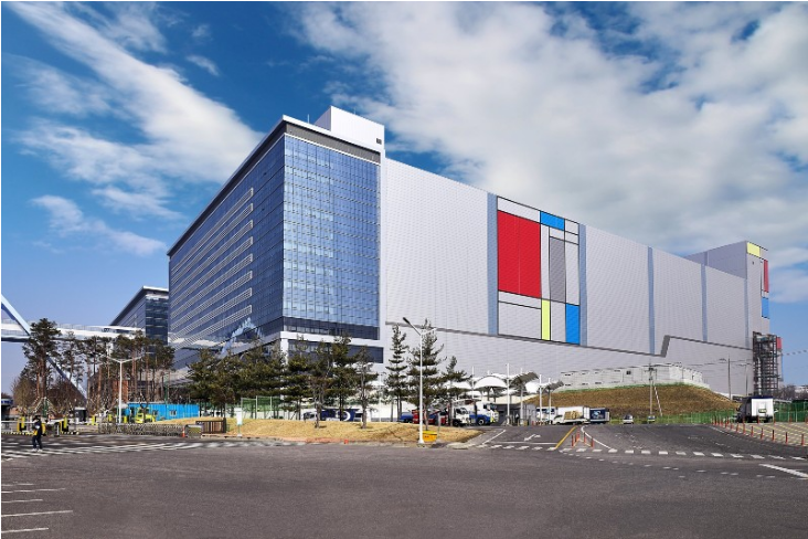
Samsung Was No. 1 in Chip Sales in Q2

发布时间:2017-07-31 00:00
作者:Ameya360
来源:Dylan McGrath
阅读量:1215

  South Korea's Samsung Electronics Co. Ltd. has unseated Intel Corp. as the world's leading semiconductor vendor, at least for one quarter.

  Samsung (Seoul) reported this week that its semiconductor division posted sales for the second quarter of 17.58 trillion won, or about $15.78 billion, besting the $14.8 billion in second quarter sales that Intel reported Thursday (July 27).

  Analysts have been saying since early this year that Samsung could rise to No. 1 in chip sales in 2017, surpassing Intel, was had led the semiconductor industry in sales every year since 1992. The booming memory chip market, which is led by Samsung, is driving growth for Samsung and other memory vendors at a faster pace than makers of logic chips.

  Market research firm IC Insights Inc. noted in May that the passing of the torch could occur in the second quarter, based on the second quarter forecasts issued by the two chip giants.

  It's unclear how long Samsung can retain the top spot in chip sales. The market for memory chips is notoriously cyclical. Growth in sales for DRAM and flash memory chips has begun to slow, and analysts forecast that a downturn in memory may be looming late next year of in 2019 as new capacity comes online and new Chinese competitors enter the fray.

  However, Bill McClean, president of IC Insights, said in an email exchange with EE Times, that Samsung is likely to grow chip sales faster than Intel on average and may well have a handle on the No. 1 spot for at least the foreseeable future.

  Given its size and product mix, Intel will most likely grow at or near the growth rate of the total semiconductor market excluding memory, roughly 5 to 6 percent per year, McClean said. "Given that there are only 3 DRAM players left and Samsung is so strong in 3D NAND flash, Samsung on average is likely to grow slightly faster than the overall market over the next few years," McClean said. “While the memory market is still cyclical and could cause Samsung to drop below Intel once again in annual sales, the trend over the long term is likely to see Samsung at the top of the ranking more often than not."

  McClean also noted that the larger chip vendors are capturing more of the overall market today than in years past, with the top 10 chip vendors holding 58 percent of the market in the first half of this year.

  Intel’s sales in 2016 represented 15.6 percent of the total semiconductor market. In 1993, Intel was the No. 1 chip vendor with 7 percent market share and in 2006 it had 11.9 percent market share, McClean said.

  "In contrast, Samsung's share was 2.8 percent in 1993, 7.4 percent in 2006 and 12.1 percent in 2016," McClean said. "So, it seems like Samsung surpassing Intel as No. 1 has more to do with Samsung gaining market share than Intel losing market share."

  Samsung's strong chip sales lifted the conglomerate's overall profit in the second quarter to 14.1 trillion won (about $12.6 billion), the highest ever quarterly profit for the nearly 80-year-old company. Nearly 60 percent of Samsung's second quarter profit came from the semiconductor division.

(备注:文章来源于网络,信息仅供参考,不代表本网站观点,如有侵权请联系删除!)

在线留言询价

相关阅读
[News] Samsung Fails to Secure Qualcomm’s 3nm Orders for the Coming Year, Dual Foundry Strategy Postponed
  According to TechNews’ report, TSMC and Samsung fiercely compete in the semiconductor foundry sector. Earlier market reports suggested that Qualcomm’s Snapdragon 8 Gen 4 mobile processor might adopt a dual-foundry strategy with TSMC and Samsung manufacturing simultaneously.  However, according to the latest industry information, due to Samsung’s conservative expansion plan for next year’s 3nm production capacity and unstable yields, Qualcomm has officially canceled the plan to utilize Samsung for next year’s processors. The dual-sourcing model is now postponed until 2025.  Samsung began mass production of its first-generation 3nm GAA (SF3E) process at the end of June last year, marking Samsung’s initial use of the innovative GAA architecture for transistor technology. The second-generation 3nm process, 3GAP (SF3), will utilize the second-generation MBCFET architecture, optimizing it based on the foundation of the first-generation 3nm SF3E. It is expected to enter mass production in 2024.  The dual-foundry strategy for Qualcomm was initially leaked by the reputable source Revegnus via the X platform (formerly Twitter). It was mentioned that the Snapdragon 8 Gen 4 processor would adopt TSMC’s 3nm (N3E) process, while Samsung’s 3GAP process would be used for the Snapdragon 8 Gen 4 supplying Samsung’s Galaxy series smartphones. Other sources suggested that due to limited capacity at TSMC’s 3nm production, Qualcomm had to seek Samsung as an alternative chip foundry.  As a result, Qualcomm originally anticipated dual-foundry production with both TSMC and Samsung in 2024, with hopes of being the first customer for the 3GAP process. However, considering Samsung’s conservative 3nm production capacity plan for next year and the instability in yields, Qualcomm decided to scrap the plan and exclusively rely on TSMC, pushing the dual-foundry strategy to 2025.  Currently, TSMC’s 3nm process technology capacity is on the rise, with expectations that by the end of 2024, monthly production capacity will reach 100,000 wafers, and the revenue contribution will increase from the current 5% to 10%.
2023-12-01 14:48 阅读量:1932
Samsung cuts NAND flash memory production
Samsung is developing next-generation memory chips for large-scale AI applications such as ChatGPT
  The large-scale application of ChatGPT and other AI chatbots will not only improve the application experience of introducing related technologies, but also bring new development opportunities to several fields, memory chip is one of them. Ameya360 reports that Samsung Electronics is exploring business opportunities by developing customized next-generation memory chips for large AI applications, such as ChatGPT, which is gaining popularity around the world.  The actual impact of ChatGPT on the chip circuit is mainly shown as follows: ChatGPT is based on Transformer technology. With the continuous iteration of the model and the increasing number of layers, the demand for computing power is increasing. Secondly, the three conditions for the operation of ChatGPT, namely, training data + model algorithm + computing power, require large-scale pre-training on the basic model. After three iterations of ChatGPT, the number of references increased from 117 million to 175 billion, and the amount of training increased significantly.  The New Computing business team of Samsung's memory business division is developing a customized next-generation memory for large-scale AI related to ChatGPT. The new computing business team, headed by Kim Jin-hyeon, is known to be a pioneer In the development of a business within the storage business division. Previously, the team focused on the development of Processing In Memory; PIM). Pims can not only store data, but also integrate and calculate data in memory, which can improve the efficiency of data processing and power consumption. Therefore, PIMs are suitable for AI.  In addition, some semiconductor industry insiders pointed out that although traditional AI chips occupy the mainstream at present and AI-dedicated chips are booming, they have met their physical limits, and the future of AI chips may be quantum chips.  Park Seong-soo, a senior researcher at the Quantum Technology Research Center at the Electronics and Communications Research Institute, said ChatGPT can also be used with a lot of computing resources, but if combined with future quantum computers, it will become a more intelligent artificial intelligence.  According to Gartner's report, total global semiconductor revenue in 2022 was approximately $601.7 billion, an increase of 1.1% year-on-year. Samsung's market share was 10.9 per cent. The ChatGPT scandal has created a new opportunity for Samsung to develop memory chips.
2023-02-21 11:26 阅读量:3607
Samsung Electronics Establishes LCA Verification on Product Carbon Footprint of Its Semiconductor Business
  Samsung Electronics Co. Ltd’s Life Cycle Assessment (LCA) on the product carbon footprint of its semiconductor business has achieved verification from DNV.  LCA is a methodology for assessing environmental impacts throughout the lifecycle of commercial products, processes, or services, by quantifying the amount of energy, materials, and waste discharge. In detail, on its semiconductors’ carbon footprint, Samsung’s LCA covers raw material extraction to chip manufacturing, assembling, and testing. Its results are in accordance with ISO 14040, ISO 14044 and ISO 14067 to ensure credibility and transparency.  The carbon footprint is commonly used by Samsung and its customers to recognize the environmental impact across all phases of Samsung’s semiconductor products, and can be used as a metric to track and reduce carbon emissions.  “Since 2019, we have been actively mobilizing efforts to measure and reduce the carbon emissions of our key memory and logic solutions,” said Dooguen Song, Executive Vice President of the Environment, Health and Safety (EHS) Center at Samsung Electronics. “By leveraging LCA, we will be able to support our customers to achieve their carbon neutrality, as well as becoming more transparent on the environmental impact of the semiconductors we produce worldwide.”  “As a global expert in energy and environmental certification, DNV is pleased to have partnered with and to congratulate Samsung on successfully establishing its reliable LCA.” said JangSup Lee, CEO of DNV Business Assurance Korea. “Together with global business leaders like Samsung, we will continue to take part in creating a more sustainable environment in the future.”  Since 2019, 37 of Samsung’s semiconductor products received carbon footprint accreditation from the Carbon Trust and UL, 6 of its memory products certified for carbon reduction from Carbon Trust. Samsung’s eco-conscious product portfolio includes DRAM, SSD, embedded storage, mobile SoC, mobile Image Sensor, automotive LED packages.  Leveraging its LCA established at the end of last year, Samsung will quantify the carbon footprints of chips manufactured across all of its global manufacturing, testing and assembly locations in Korea, China, and the U.S.  With sustainability at its core, Samsung will expand its LCA to include water and resource footprints to provide a more comprehensive assessment that will ultimately reduce the environmental impact of various applications such as mobile and wearables, data centers, consumer electronics, automotive, communications and more.
2023-02-13 15:12 阅读量:3159
  • 一周热料
  • 紧缺物料秒杀
型号 品牌 询价
RB751G-40T2R ROHM Semiconductor
MC33074DR2G onsemi
CDZVT2R20B ROHM Semiconductor
BD71847AMWV-E2 ROHM Semiconductor
TL431ACLPR Texas Instruments
型号 品牌 抢购
TPS63050YFFR Texas Instruments
BP3621 ROHM Semiconductor
ESR03EZPJ151 ROHM Semiconductor
BU33JA2MNVX-CTL ROHM Semiconductor
IPZ40N04S5L4R8ATMA1 Infineon Technologies
STM32F429IGT6 STMicroelectronics
热门标签
ROHM
Aavid
Averlogic
开发板
SUSUMU
NXP
PCB
传感器
半导体
相关百科
关于我们
AMEYA360微信服务号 AMEYA360微信服务号
AMEYA360商城(www.ameya360.com)上线于2011年,现 有超过3500家优质供应商,收录600万种产品型号数据,100 多万种元器件库存可供选购,产品覆盖MCU+存储器+电源芯 片+IGBT+MOS管+运放+射频蓝牙+传感器+电阻电容电感+ 连接器等多个领域,平台主营业务涵盖电子元器件现货销售、 BOM配单及提供产品配套资料等,为广大客户提供一站式购 销服务。