400mA, High Output Slew Rate: NOVOSENSE's NSOPA240x Series Cracks the Challenge of Resolvers

发布时间:2024-07-01 13:47
作者:AMEYA360
来源:novosns
阅读量:282

  With the continuous pursuit of high-precision, high-performance motor control technology, the ability of resolvers, as one of its core components, to accurately measure angular position and rotational speed becomes particularly important.

  However, the special requirements of resolver drive circuits have always been a technical bottleneck in the development of the industry. To address this challenge, NOVOSENSE recently released the new NSOPA240x series of operational amplifier, which is designed to simplify circuit design and improve system robustness, bringing innovative solutions to resolver drive applications.

  As electromagnetic sensors that can be used to accurately measure angular position and rotational speed, resolvers are widely used in industrial motor controls, servos, robots, and powertrain units in electric and hybrid vehicles. Particularly in electric vehicles, resolvers provide motor control algorithms with precise and stable position information, which is critical to ensuring ideal performance in a wide range of driving conditions. Through their unique operating principle, resolvers provide real-time and accurate feedback on the rotor angle and speed, enabling electric vehicles' motor control algorithms to accurately adjust the current output for smooth driving and instant response. In addition, resolvers' high temperature resistance, simple and reliable mechanism, compact size and low cost make them adaptable to the compact design requirements of electric vehicles and reduce overall costs.

  In practice, the design of resolver drive circuits faces multiple challenges. First, the requirements for high current output and high slew rate must be met to ensure a stable excitation signal for resolvers. Second, simplifying circuit design and improving system robustness are also important issues faced by engineers. In addition, complex noise environments and stringent safety requirements bring more difficulties to the design.

  With their excellent high gain bandwidth and slew rate, as well as continuous high output current drive function, NOVOSENSE's NSOPA240x high-current output operational amplifiers meet the stringent requirements of resolver primary coils for low-distortion and differential high-amplitude excitation. More importantly, NSOPA240x integrates internal thermal shutdown and overcurrent production, which not only optimizes the circuit design and reduces the system cost, but also significantly improves the overall system reliability and performance.

  The automotive version of the NSOPA240x series meets the reliability requirements of AEC-Q100 Grade 1 and can work in harsh environments of -40~125°C. Different channel versions are available to meet different customer needs, with TO252-5 package for single-channel and HTSSOP14 package for dual-channel, as shown in the table below.

400mA, High Output Slew Rate: NOVOSENSE's NSOPA240x Series Cracks the Challenge of Resolvers

  High current output capability - adapt to various resolver primary coil drives

  Output current capability and output swing are among the most important indicators to measure the driving capability of power amplifiers. The relationship between load current and output swing directly determines the dissipated power in driving operational amplifiers. The excitation primary coil of a resolver usually has a very low DCR (DC resistance), typically less than 100Ω, so a strong current output capability up to 200mA is required to drive the coil. NSOPA240x is designed with a maximum continuous output current capability of 400mA, fully meeting the drive requirements of various resolvers.

  High output slew rate - ensure undistorted primary coil excitation signal

  Slew rate is one of the most important performance indicators reflecting the dynamic response of an operational amplifier, and the minimum requirement for undistorted sinusoidal signals is shown in the following formula:

400mA, High Output Slew Rate: NOVOSENSE's NSOPA240x Series Cracks the Challenge of Resolvers

  Different types of resolvers have different requirements for the amplitude and frequency of the excitation signal. Taking a 7Vrms, 10kHz excitation signal as an example. According to the calculation results of the above formula, the minimum slew rate required to ensure no distortion is about 0.6 V/μs. With a slew rate of 5.5 V/μs, NSOPA240x meets most application requirements for resolver drives.

  Integrated current limiting protection and overheating protection - improve resolver system reliability, and reduce complexity and cost

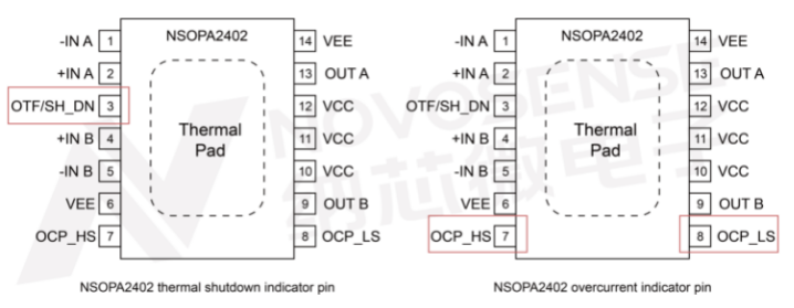
  For the power level of several hundred mA at the primary drive end of a resolver, perfect protection measures must be taken, otherwise the system will be seriously threatened or even burned due to overheating and other reasons. NSOPA240x integrates a thermal shutdown protection function. When the chip junction temperature exceeds 173°C, the device will be disabled and the occurrence of a thermal shutdown event will be indicated by the OTF/SH_DN status. To prevent repeated triggering, the overtemperature shutdown function has a temperature hysteresis, where the junction temperature needs to fall back to 155°C before the device is re-enabled and the state of the OTF/SH_DN pin changes to indicate that the thermal shutdown event has stopped.

  As shown in the figure below, NSOPA240x can provide customers with system-level functional safety and simultaneously indicate short circuit to power and short circuit to ground.
400mA, High Output Slew Rate: NOVOSENSE's NSOPA240x Series Cracks the Challenge of Resolvers

  In addition, each operational amplifier in the chip has current limiting protection for the PMOS (high side) and NMOS (low side) output transistors, because overcurrent may be found on the high side or the low side. And two dedicated pins (as shown in the red box in the figure) are provided to distinguish between high side overcurrent and low side overcurrent, corresponding to the applications of short circuit to ground and short circuit to supply voltage respectively. When the output current returns to normal, the indicator pins will be released synchronously, allowing the system to easily cope with short circuit test scenarios similar to those specified in the ISO 16750 standard.

(备注:文章来源于网络,信息仅供参考,不代表本网站观点,如有侵权请联系删除!)

在线留言询价

相关阅读
NSM211x Series High-Precision AEC-Q100 Current Sensors Eliminate Need for External Isolation Components
  NOVOSENSE Microelectronics, a semiconductor company specializing in high-performance analog and mixed-signal chips, has announced the NSM211x, a series of automotive-grade fully integrated high-bandwidth, high-isolation current sensors that both ensure precise current measurement and eliminate the need for any external isolation components.  On display at Electronica 2024 (Stand B5.450), the automotive-grade series targets applications including OBC/DC-DC converters, PTCs, automotive motor control, charging station current detection and fuel cell systems.  Certified to meet AEC-Q100 Grade 0 reliability standards, the series is designed to operate stably within a wide temperature range (-40 to 150°C) and addresses the needs of AC or DC current detection in automotive applications with a high isolation voltage, strong current handling capability and high reliability.  With a -3 dB bandwidth of up to 1 MHz and a response time of 400 ns, the NSM211x series helps control systems achieve rapid loop control and overcurrent protection. The series also features a creepage distance of up to 8.2mm and isolation voltage withstand of 5,000 Vrms per UL standards, with a maximum working isolation voltage of 1,618 Vpk.  It is available in three packaging options, SOP8, SOW16 and SOW10. These respectively have a primary side impedance of 1.2 mΩ, 0.85 mΩ/1 mΩ and an industry leading 0.27mΩ, with a continuous current handling capability of up to 100 A. Multiple product models are available for each package.  The current sensors integrate internal temperature compensation algorithms and offline calibration to enable a high measurement accuracy (<±2% sensitivity error and <±10 mV offset error) across the full temperature range, with no need for secondary programming.  The NSM211x series supports 3.3 V and 5 V power supply voltage as well as DC or AC current measurement with a current range of 5~200 A with options for reference voltage output, overcurrent protection output, and configurable overcurrent protection thresholds.
2024-11-15 14:30 阅读量:259
novosns:Technical Sharing | The Introduction of Gate Drivers and the Applications
  1) Introduction of the Gate Drivers  Gate driver is a buffer circuit between the low-voltage controller and the high-power circuit, which is used to amplify the control signals of the controller for more effective turn-on and turn-off of power devices.  1. The functions of gate driver are as follows  - Gate driver can convert the low-voltage signal from the controller to higher-voltage drive signal, so as to achieve stable turn-on and turn-off of power devices.  - Gate driver can provide transient source and sink peak currents, which can improve the switching speed of power devices and reduce the switching loss.  - Gate driver can effectively isolate the noise of high-power circuits and protect sensitive circuits against interference.  - Gate driver typically integrates protection functions to effectively prevent damages to power devices.  It can be seen that gate driver is used to ensure better performance of power devices in the system.  2. There are four types of common power devices  - Si-MOSFET devices, which withstand voltage of 20V-650V and are suitable for low-power systems.  - Si-IGBT devices, which withstand voltage of greater than 650V and provide a strong current endurance capability. This type is suitable for high-voltage and high-power systems.  --- Both Si-MOSFET and Si-IGBT are Si-based power devices that have been widely used, and their manufacturing technologies are mature and stable.  - SiC-MOSFET devices, which provide withstand voltage range comparable to IGBT, but feature fast switching speed and low switching loss. They are more suitable for high-voltage and high-power systems.  - GaN devices, currently constrained by the manufacturing technology, typically have a withstand voltage of less than 650V, but provide obviously advantageous switching performance. This power device type is suitable for high-frequency and high-power systems.  --- SiC-MOSFET and GaN devices are wide bandgap semiconductors that boast significant performance advantages over Si-based ones, and will have a broad range of applications in the future.  3. NOVOSENSE gate drivers  Different power devices have varied requirements for gate drivers. Currently, NOVOSENSE has developed driver products suitable for these four types of power devices.  4. Switching process of power devices  How does a gate driver control the turn-on and turn-off of power devices? Below is a detailed explanation of the switching process of power devices. In power devices, there are equivalent parasitic capacitances, such as CGS, CGD and CDS. The switching process of a power device can be equivalent to the charging and discharging process of its parasitic capacitances.  4.1 Turn-on process  In the turn-on process, the driver IC connects the output signal to the driver power supply through an internal source current MOS, and charges CGS and discharges CGD through a gate resistor.  - (t0-t1) stage: The gate current charges CGS, and VGS gradually increases. At this point, the power device is still turned off.  - (t1-t2) stage: When VGS increases to a value greater than the gate threshold voltage Vth, the power device begins to turn on, and IDS increases with VGS until it reaches the maximum value.  - (t2-t3) stage: This is the Miller Plateau period, where the gate current mainly discharges CGD, and VDS begins to decrease. The device is fully turned on.  - (t3-t4) stage: The gate current continues to charge CGS, and VGS gradually increases to the power supply voltage. When the gate current reduces to zero, the turn-on process ends. The turn-on loss of the power device mainly occurs at the t1-t3 stage.  4.2 Turn-off process  In the turn-off process, the driver IC connects the output signal to the GND through an internal sink current MOS, and discharges CGS and charges CGD through a gate resistor.  - (t0-t1) stage: The gate current mainly discharges CGS, and VGS gradually decreases.  - (t1-t2) stage: This is the Miller Plateau period, where the gate current mainly charges CGD, and VDS begins to increase. When the voltage reaches VDC, the Miller Plateau ends.  - (t2-t3) stage: IDS begins to decrease. When VGS decreases to Vth, IDS drops to zero, and the power device is completely turned off.  - (t3-t4) stage: The gate current continues to discharge CGS, and VGS eventually drops to zero. The turn-off process ends. The turn-off loss of the power device mainly occurs at the t1-t3 stage.  It can be seen from the analysis above that shortening the t1-t3 stage can effectively reduce the switching loss of power devices.  4.3 Three types of common driver IC  At present, there are three types of commonly used driver ICs, namely non-isolated low-side drivers, non-isolated half-bridge drivers, and isolated drivers.  - Non-isolated low-side drivers are only suitable for power devices with a reference to GND, and provide dual-channel or single-channel driving capability. Non-isolated drivers are relatively simple to implement, requiring only single power supply. They are mainly used in low-voltage systems, such as AC/DC converters, electric tools, and low-voltage DC/DC converters. Currently, NOVOSENSE offers non-isolated low-side driver ICs including NSD1026V and NSD1015.  - Non-isolated half-bridge drivers are used in power systems with a half-bridge configuration. The withstand voltage of the high and low sides is usually achieved through level shifting or isolation, ranging from 200V to 600V. To prevent shoot-through, half-bridge drivers provide an interlock function. When a non-isolated half-bridge driver is used in a system, single power supply plus bootstrap power is typically adopted. This driver IC type is mainly used in low-voltage or high-voltage systems, such as AC/DC converters, motor drives, and on-board DC/DC converters. Currently, the half-bridge driver ICs from NOVOSENSE include NSD1624 and NSD1224.  - Isolated drivers use an internal isolation barrier to physically isolate high and low voltages. Isolated drivers provide flexibility in application. Single-channel and dual-channel isolated drivers are available for low-side, high-side, or half-bridge applications. To achieve primary and secondary isolation in the system, the high-voltage side requires an isolated power supply, making the power supply system relatively complex. Isolated drivers are mainly used in high-voltage systems, such as electric drives, photovoltaic inverters, and OBCs. Currently, NOVOSENSE offers NSI6602 dual-channel isolated driver IC, NSI6601/NSI6601M single-channel isolated driver IC, NSI6801 opto-compatible isolated single-channel driver IC, and NSI6611/NSI68515 smart isolated driver IC.  2) Introduction to Isolation Solutions  In a high-voltage power system, there is usually isolation between high voltage and high voltage, as well as between high voltage and low voltage. Why is isolation driver needed? First, an isolated driver can avoid harm to human body caused by high-voltage electricity, and meet safety standards through isolation. Second, it can protect the control system from damages that can be caused by lightning strikes and high voltage transients. Third, an isolated driver can eliminate ground loops and reduce interference from the high voltage side to the low voltage side. Fourth, it can realize voltage or current change and energy transfer.  There are three commonly used isolation schemes. The first is optocoupler isolation, which achieves signal transmission through light-emitting diodes and phototransistors. This isolation scheme is low-cost, but provides weak CMTI (Common Mode Transient Immunity), limited temperature range, and short service life. The second isolation scheme is magnetic isolation, where the chip integrates micro-transformer and electronic circuit to achieve signal transmission. The magnetic isolation chips deliver benefits such as long lifetime, wide temperature range, and strong CMTI, but involve complex technology, high cost, and prominent EMI issue. The third isolation scheme is capacitive isolation, which achieves signal transmission through isolation capacitors and electronic circuits. It usually uses silicon dioxide (SiO2) as the insulating material. The capacitive isolation scheme features low cost, long isolation life, wide temperature range, and strong CMTI. NOVOSENSE adopts the capacitive isolation scheme.  NOVOSENSE isolation solution  Isolated driver ICs from NOVOSENSE usually have two dies – the primary die on the input side and the secondary die on the output side. There is a physical isolation between the dies. Two isolation capacitors are connected in series on the die to achieve double insulation capability. If one of the dies experiences an EOS failure, the driver IC can still maintain basic insulation capability. The top and bottom substrates of the two isolation capacitors are insulated using SiO2, which can ensure stable material properties, good chip consistency, and long isolation life. The top substrates of the two isolation capacitors are connected by metal wires for signal transmission. NOVOSENSE’s isolated driver ICs can withstand surge voltage up to 12kV and 8kV transient insulation voltage test, far exceeding the insulation requirements of high-voltage systems.  The communication between the dies adopts the differential OOK modulation scheme, which ensures stable and reliable communication. The input signal is modulated at a high frequency and then transmitted from the primary die to the high-voltage die through the isolation capacitor, with the modulation frequency at a level of over 100 MHz. A proprietary CMTI modular circuit is added at the input side of the differential signal, allowing the IC to achieve a stronger CMTI capability up to 150V/ns. For power systems with a high dv/dt, the IC can still work stably without abnormal wave emission.
2024-06-21 11:23 阅读量:522
On the Fast Lane: NOVOSENSE's Ongoing Commitment to Automotive Chip Excellence
  Automobiles are undergoing increasing electrification and digitalization, from electric drive trains to immersive infotainment systems in the cockpit.  NOVOSENSE, a pioneering force in the automotive chips, recently unveiled several groundbreaking products aimed at enhancing performance, reliability, and efficiency in automotive applications.  NCA1462-Q1, an automotive-qualified CAN SIC based on innovative ringing suppression patent  NCA1462-Q1 is based on its proprietary innovative ringing suppression patent. Compared with CAN FD solution, NCA1462-Q1 is further compatible with the CiA 601-4 standard on the premise of meeting the ISO 11898-2:2016 standard, and can achieve a data rate of ≥8Mbps. With NOVOSENSE's patented ringing suppression function, NCA1462-Q1 maintains good signal quality even in the case of star network multi-node connection; in addition, its ultra-high EMC performance and more flexible VIO as low as 1.8V can effectively help engineers simplify system design and create high-quality automotive communication system.  NSHT30-Q1, a relative humidity (RH) and temperature sensor based on CMOS-MEMS  NSHT30-Q1 integrates a complete sensor system on a single chip, including a capacitive RH sensor, CMOS temperature sensor and signal processor, and an I2C digital communication interface. It is designed in DFN package with Wettable Flank, and the product size is 2.5mm×2.5mm×0.9mm. NSHT30-Q1's I2C interface features two selectable addresses with communication speed up to 1 MHz and supports a wide supply voltage range of 2.0V~5.5V.  NSOPA9xxx series, general-purpose operational amplifiers for automotive applications  NSOPA9xxx series is suitable for 40V high voltage and offers a variety of product models with bandwidth option of 1MHz/5MHz/10MHz and 1/2/4-channel. It meets the reliability requirements of AEC-Q100 Grade 1, and can operate from -40°C to 125°C. Different package versions are available to meet different customer needs: SOT23-5, SOP-8 for 1-channel; MSOP-8, SOP-8 for 2-channel; and TSSOP-14, SOP-14 for 4-channel.  NSD3604/8-Q1, a new automotive-qualified 4/8-channel multi-channel half-bridge driver  NSD3604/8-Q1 can drive multiple loads and is used in automotive domain control architecture. It covers 4/8-channel half-bridge drive which can drive 4 DC brushed motors, and achieve multi-channel high-current motor drive, and also be used as a multi-channel high-side switch drive. NSD3604/8-Q1 is suitable for multi-motor or multi-load applications, such as car window lifting, electric seats, door locks, electric tailgates, and proportional valves and other body control applications.
2024-04-17 13:24 阅读量:540
novosns:Must-Know Basic Facts about Digital Isolators
  Electrical isolation is a crucial concept in the design of electrical systems. Through the isolation of the high and low voltage systems, the following important functions can be achieved:  1.Make the high and low voltage systems independent of each other and improve the anti-interference capability of the low voltage system;  2.Ensure safe interaction between the high and low voltage systems so that the systems can work safely;  3.Protect users' personal safety by avoiding electric shock from the high voltage.  In this Technical Sharing, the basics of electrical isolation will be introduced in detail, including: the definition and importance of electrical isolation, the classification and definition of isolation levels, and the standards and specifications for isolator certification.(Click here to watch the video  Definition and Importance of Electrical Isolation  Electrical isolation uses isolators to prevent destructive electrical signals from being transmitted between high/low voltage subsystems, while allowing safe electrical signals required for system operation to interact between high/low voltage systems. Three system interaction scenarios are discussed below:  1.When two low voltage systems interact, electrical signals can be freely transmitted between the two systems. In this state, we usually consider the systems to be working safely.  2.When high/low voltage systems interact directly without isolators, due to the high potential difference between the high voltage system and the low voltage system, the high voltage system may transmit destructive electrical signals to the low voltage system, which will cause the low voltage system to malfunction and even cause permanent damage to the low voltage system. This will not only affect the functional safety of the systems, but also endanger personal safety and lead to major safety accidents.  3.After using an isolator for electrical isolation between the high and low voltage systems, destructive electrical signals are blocked by the isolator. Safe electrical signals required for normal system operation interact between the high and low voltage systems, ensuring the functional safety of the systems.  Classification and Definition of Isolation Levels  Based on different isolation performance, electrical isolation is divided into different isolation levels. Functional isolation, basic isolation, dual isolation, and reinforced isolation are among typical isolation levels:  1. Functional isolation can only achieve the isolation necessary for normal device operation and does not have the function of electric shock protection, such as the PCB materials on the circuit boards.  2. Basic isolation only provides single-stage isolation and can achieve isolation while the insulation layer is intact. But once the insulation layer fails, the system will be at risk of electric shock. Under normal circumstances, the isolation voltage that basic isolators can isolate is around 3kV, and there are a few basic isolators whose isolation voltage can reach 5kV.  3. Dual isolation adds a layer of isolation on the basis of basic isolation to achieve system redundancy. It can ensure system security when single-stage isolation fails. In this way, the isolation voltage can reach 5kV and above.  4. Reinforced isolation is also single-stage isolation, but it can achieve the same isolation strength as dual isolation.  Standards and Specifications for Isolator Certification  Currently, most common isolators adopt basic and reinforced isolation. In order to be certified for the two isolation levels, the performance of isolators needs to comply with regional codes and safety standards.  In terms of isolator standards and certifications, the International Electrotechnical Commission (IEC) is the earliest non-governmental international electrotechnical standardization organization in the world. IEC works with organizations in multiple regions to develop international safety standards for electrical/electronic devices. In different regions, local standards are developed by different organizations. For example, the United States, Canada, Germany, and China all have local organizations.  Isolators must meet local standards before they can be legally marketed commercially and the electrical/electronic products fitted with them can be sold to customers. Typically, the first page of an isolator datasheet will list standards that the isolator has passed. The reinforced isolation level of digital isolators is mainly proposed by VDE and promoted by IEC as a global standard. NOVOSENSE is a leader of digital isolators in China and also the first semiconductor company to obtain the VDE enhanced isolation certification.  Under the current VDE standards, both basic and reinforced isolators have corresponding test standards and parameter specifications.  In the maximum surge voltage test, both basic and reinforced isolators are required to pass 50 bipolar surge impulses, and the final measured voltage must not exceed 1.3 times the maximum surge voltage in the datasheet, on top of which reinforced isolators are required to pass a surge voltage test of at least 10kV.  In applications, partial discharge phenomenon occurs when there are defects inside a device. which does not affect the insulation strength in short time. However, under the repeated impact of high voltage, the defect will eventually lead to the breakdown of the isolation barrier. Therefore, these defects need to be detected through non-destructive testing. Basic isolators need to pass the 1.5 times VIOSM surge test, while partial discharge testing of reinforced isolators needs to be conducted at 1.875 times VIOSM voltage.  According to the working life of chips at different temperatures and voltages, the working voltage of chips under the minimum rated life and failure rate during the target life can be fitted by Weibull distribution, and then VIORM and VIOSM can be obtained according to the requirements of the VDE correlation coefficients. It can also be seen from the table that reinforced isolators have a longer working life and a lower failure rate during their life.  After passing the above tests, isolators are deemed to have met the requirements for VDE certification.  To sum up, electrical isolation involves the working safety of devices and the personal safety of users, and is an indispensable part of electrical system design.
2024-04-09 11:58 阅读量:576
  • 一周热料
  • 紧缺物料秒杀
型号 品牌 询价
MC33074DR2G onsemi
RB751G-40T2R ROHM Semiconductor
CDZVT2R20B ROHM Semiconductor
BD71847AMWV-E2 ROHM Semiconductor
TL431ACLPR Texas Instruments
型号 品牌 抢购
TPS63050YFFR Texas Instruments
STM32F429IGT6 STMicroelectronics
IPZ40N04S5L4R8ATMA1 Infineon Technologies
BU33JA2MNVX-CTL ROHM Semiconductor
BP3621 ROHM Semiconductor
ESR03EZPJ151 ROHM Semiconductor
热门标签
ROHM
Aavid
Averlogic
开发板
SUSUMU
NXP
PCB
传感器
半导体
相关百科
关于我们
AMEYA360微信服务号 AMEYA360微信服务号
AMEYA360商城(www.ameya360.com)上线于2011年,现 有超过3500家优质供应商,收录600万种产品型号数据,100 多万种元器件库存可供选购,产品覆盖MCU+存储器+电源芯 片+IGBT+MOS管+运放+射频蓝牙+传感器+电阻电容电感+ 连接器等多个领域,平台主营业务涵盖电子元器件现货销售、 BOM配单及提供产品配套资料等,为广大客户提供一站式购 销服务。