- Ameya360 Component Supply Platform >
- Trade news >
- Why Fabs Worry About Tool Parts
Why Fabs Worry About Tool Parts
How a single O ring can affect yield, and what to do about it.
Achieving high yields with acceptable costs is becoming much more difficult as chipmakers migrate to next-generation 3D NAND and finFET devices—but not just because of rising complexity or lithography issues.
To fabricate an advanced logic chip, for example, a wafer moves from one piece of equipment to another in what amounts to 1,000 process steps or more in a fab. Any glitch with the equipment or a process step can cause defects, thereby impacting yield. The culprit may be a malfunction in seemingly insignificant parts or sub-systems in the equipment itself.
Simply put, defects introduced by process-critical components in fab equipment can impact wafer yields, according to members from SEMI’sSemiconductor Components, Instruments, and Subsystems (SCIS) Special Interest Group, an organization that represents suppliers of components and sub-systems. The issues have been known for some time, but they are expected to become more problematic as chipmakers move to 10nm/7nm and beyond, according to SCIS. The group’s members include GlobalFoundries, IM Flash, Intel, Micron, TI and Samsung as well as major fab tool and component suppliers.
The components and sub-systems in fab equipment are taken for granted, but they play a critical role in the semiconductor supply chain. For example, the more sophisticated fab tools incorporate more than 50,000 parts from dozens of suppliers. Chambers, pumps, RF generators, seals and valves are among the key components in a tool.
Generally, the components are robust and don’t cause problems, but at times they can contribute to issues in the fab. For instance, based on real events from chipmakers, here’s just a small sample of what can go wrong in the fab:
The wrong O-rings were installed in a portion of the sub-fab, which could cause contamination in the flow. An O-ring is a part that serves as a seal in a system.
A pressure regulator malfunctions in the ultra-pure water system, causing contamination in the process.
A liner material breach occurs in a bulk chemical distribution system, causing corrosion in the unit.
“Sub-components have a major impact in facility systems, which in turn affects fab equipment performance,” said Norm Armour, managing director of worldwide facilities and corporate EHS at Micron Technology. “Our sub-component and material suppliers are doing a good job keeping up with our roadmap. But once in a while, there is a hiccup. The hiccup is what can upset the whole ecosystem.”
For that reason, the industry’s supply chain is undergoing some changes. Not long ago, equipment vendors mainly specified the tool component from suppliers. Now, in addition to tool makers, chipmakers also are involved, and they are collaborating with component vendors in an effort to prevent a potential problem from occurring in the fab.
“The moral of the story here is that you have to spec not only your fab tool components, but also your sub-components,” Armour said at a recent event at Semicon West. “We have been collaborating on the tool side for 40 years. Why not do that with the sub-component manufacturers as well?”
Collaboration is only part of the solution, however. At advanced nodes, the industry wants to perform more rigorous tests on tool components, but they also need to find a better way in terms of how defects are measured on these parts. The problem is that measurement standards are either inadequate or non-existent. For example, there are few, if any, standard specs in the IC industry for O-ring seals, which were originally developed for steam engines in the 1800s.
Seeking to address these issues, SEMI’s SCIS Special Interest Group is establishing new standards and methods for measuring defects introduced by components. In addition, there are other solutions to solve the problem, such as advanced metrology, wafer monitoring and simulation techniques.
Fab challenges
Today’s fabs have a number of moving pieces. According to UC Berkeley, a theoretical fab with 50,000 wafer starts per month requires the following equipment:
50 scanners/steppers plus wafer tracks;
10 high-current and 8 medium-current ion implanters;
40 etch machines, and
30 CVD tools.

Fig. 1: Inside a fab. Source: GlobalFoundries
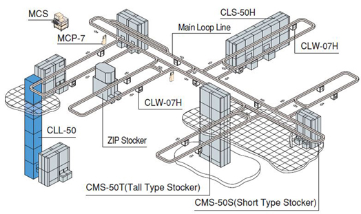
In addition, 300mm fabs are also automated plants that make use of an assortment of automated material handling systems and wafer transport mechanisms.

Fig. 2: Unified fab transport system. Source: Daifuku
In the fab, the tools must process smaller and more exact features. And at each node, the defects are becoming smaller and harder to find, thereby requiring new and advanced metrology techniques. “We are shrinking the area of a circuit by 50% every generation,” said David Fried, chief technology officer at Coventor. “You are going to have 30 different metrology techniques in the fab.”
At times, though, the fab flow encounters a problem. Defects can crop up in any part of the process. Then, a tool can run into a problem in the fab, which could mean any number of issues.
Generally, a fab tool incorporates various sensors. The sensors monitor several functions in the tool, such as the gas flow, temperature, pressure and RF power. “Every tool has hundreds, if not thousands, of sensors,” Fried said. “Each has an acceptable range. If a tool sensor detects a fault, it usually (triggers an) alarm and takes itself off the automatic dispatch system so that no more lots of wafers will be sent to the tool for processing.”
Other issues can also crop up. “After most process steps, measurements or metrology operations are performed to measure the success of the process,” he said. “If those measurements are out of spec, the lot is held for further evaluation. But this can lead to the preceding process tool being taken down for maintenance or further testing.”
Still, the goal is to keep the fab up and running without a stoppage. “There is never a step in the process where wafers must go through one tool,” he said. “In any fab, there are many of the same tools to permit high-volume manufacturing to flow through the factory, even with ‘tool-downs.’”
Regardless, fab tools require maintenance. Every tool has a preventive maintenance plan where the system is taken offline for cleaning and upgrades. So the fab keeps spare parts on hand.
“Some fabs do their own maintenance, which are groups often called ‘Equipment Engineering,’” he said. “Many fabs buy their tools with ‘vendor maintenance contracts,’ which means if the tool goes down for unexpected reasons, the vendor is required to come to service it. These are stressful times for both parties.”
Indeed, if a tool has an issue, it’s sometimes an arduous task to troubleshoot and fix the problem. It can be a time-consuming and costly process as well.
For example, a component could not only malfunction in a tool, but it could cause a possible process-induced defect. The number of components varies from tool to tool, but the more sophisticated systems have a staggering number of parts. Consider Zeiss’ AIMS line of photomask inspection tools for extreme ultraviolet (EUV) lithography applications. The system consists of 4,500 sub-systems and 64,000 individual parts from 134 different suppliers, according to data from Intel. The AIMS tool is one of the more advanced systems in the market, but it exemplifies the complexity of today’s tools.
Hypothetically, if the AIMS tool has an issue in the field, there might be a problem with one or more parts in the system. Finding them is a difficult task. “If we are chasing a defect on the tool, we are looking for a needle in a haystack,” said Ya-hong Neirynck, a technology enabling specialist at Intel.
Potential issues with the components give chipmakers just one more thing to worry about in an already complicated supply chain and process flow in the fab. “You have more numbers of variables that can impact your wafer,” said Pawitter Mangat, director of global incoming quality at GlobalFoundries. “Tracking those variations, tracking those components and (tracking the) traceability of processes all lead into those variables. We cannot afford to have parts that don’t sustain the performance. Think about this in terms of the cost and the qualifications we have to go through every time an O-ring is changed and the validation.”
And as chipmakers move to 10nm/7nm and beyond, there is no margin for error in the fab. “The variations have to be controlled,” Mangat said. “The message is that some of these variations that we see from processes over time are no longer going to be the norm for advanced nodes, which require a lot more rigorous controls, spec limits and operations.”
There is hope, however. On the components/sub-systems front, Mangat listed several solutions for the industry:
More collaboration in the supply chain.
Bolster the quality programs for component suppliers.
Develop baseline metrics and defect testing standards for components.
Devise ways to trace the problem.
Boosting collaboration
The process starts when a tool maker develops a new system. From there, an equipment maker procures components for the system.
Over the years, tool makers have developed a list of preferred component suppliers who they know and trust. They also know which suppliers to avoid.
Even chipmakers keep tabs on suppliers. “We follow a very stringent internal SOP to ensure that our parts and sub-systems meet quality standards,” according to officials from UMC. “The measures include inspection for safety, hardware performance and ensuring that the delivered output is in line with the required specifications. Keeping an independent qualification process within UMC enables us to set our own rigorous quality benchmarks as well as control the parameters and conditions involved in qualifying incoming tools or materials.”
Obviously, vendors must do their homework. They must understand the characteristics of a given component so they can anticipate a potential problem before it occurs in the fab.
“It varies depending on the supplier,” said Kirk Hasserjian, vice president of service product development at Applied Global Services for Applied Materials. “Some of these technologies are very sensitive to certain types of defects. Others technologies are much less sensitive. CMOS image sensors are a classic example. They are extremely sensitive to metal containments and trace metals.”
In addition, tool makers must continue to re-emphasize the need for quality among their suppliers, and for good reason. “The technology changes,” said Aki Sekiguchi, vice president and general manager of the Advanced Semiconductor Technology Division at Tokyo Electron Ltd. (TEL). “What is okay for 10nm may not be good for 7nm, 5nm and so forth. In general, as the technology gets tighter and tighter, the specs are tighter.”
There are some limitations, however. It makes sense to implement more rigorous controls and testing for the critical components. It’s impossible to implement the same controls for every part because it’s too expensive.
Yet every part must meet spec. So tool vendors and their component suppliers must strike a balance between how much a part is tested versus cost. “There is an associated cost,” Sekiguchi said. “If you really take control over every single component, the economic format breaks down.”
Component suppliers attempt to provide the best solutions, but in general they are unaware of the exact conditions or recipes that their products are subjected to during the actual process. Sometimes chipmakers and tool vendors don’t want to reveal their key intellectual property to suppliers.
One of the drawbacks of the traditional way of doing business is that the part may fail and the supplier has no idea, or only a vague inkling, why it didn’t meet spec. The obvious solution is collaboration. For this, the various parties must get more involved in the product development process.
The challenge is when the parties need to share IP. Sharing IP on basic parts is simple. But companies are much more cautious about revealing IP on the more critical components, such as process chambers.
To solve these issues, the industry must find a happy medium. “There has to be a balance,” Sekiguchi said. “You have to strike a balance between the amount of information that you share and the kinds of information you share.”
The components require more rigorous characterization and testing as chipmakers migrate to more advanced nodes. But how that gets accomplished isn’t clear.
“To date, there is no industry alignment on how defects are measured on various components and sub-components and on how these results are reported,” said Paul Trio, senior manager of strategic initiatives at SEMI.
Take an O-ring for example. An O-ring is a small item that fits between two or more parts, which forms a seal at the interface. Each fab tool has several different seal types, including those for the lids, ports and windows. But each seal vendor develops proprietary products. Therefore, each vendor has different and proprietary data about their products, but there is no standard way to test or package these items.
“The problem is the same spec that was invented for the steam engine is the same spec they use for these seals today. Therein lies the problem. There is no spec,” said Dalia Vernikovsky, chief executive of Applied Seals North America and co-chair for SCIS.
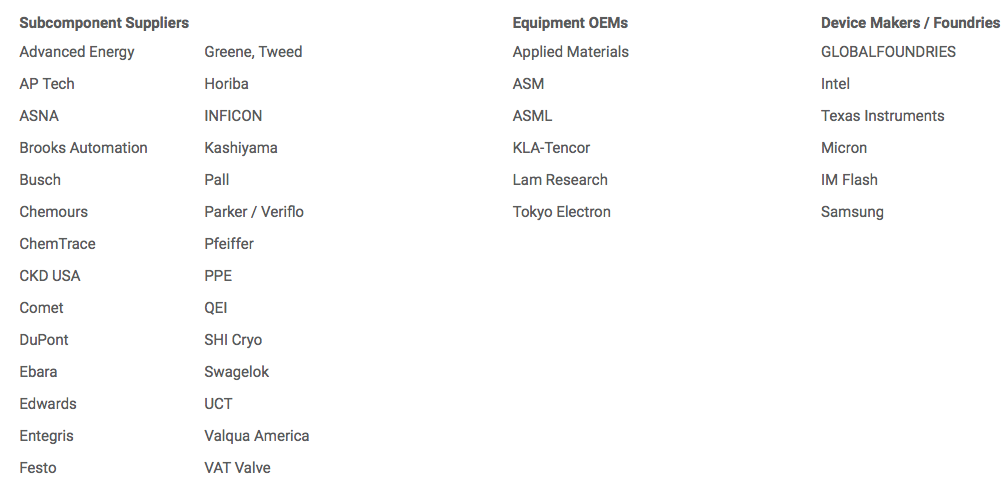
Many other types of components are in the same boat, prompting the need for standards. So in 2013, SEMI and others launched SCIS. Besides major chipmakers, Applied Materials, ASMI, ASML, KLA-Tencor, Lam and TEL are members of SCIS as well as a number of component vendors.

Fig. 3: Participating Companies in SCIS. Source: SEMI
SCIS’ charter is to get chipmakers, tool vendors and parts suppliers in the same room and hammer out “a baseline for measuring defects introduced by process-critical components,” according to SEMI.
“The first two years was really spent working on test methods for seal impurities,” SEMI’s Trio said. “SCIS has since expanded to other critical components.”
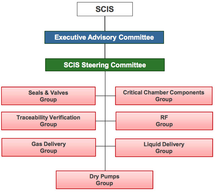
Today, SCIS has eight working groups in the following areas—chambers; gas delivery; liquid delivery; pumps; RF generators; seals; and valves. The eighth group, the Traceability Verification Group, is developing an “Information Exchange Model.” This involves providing traceability data to a potential issue in the fab via the cloud.

Fig. 4: SCIS Organizational Structure. Source: SEMI SCIS
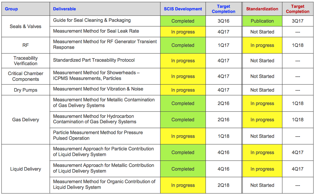
So far, the group has made progress on several fronts. “It depends on the type of components we are talking about. The industry should come together on the simpler ones, such as valves, pumps, seals, sub-fab areas and abatement,” Applied Seals’ Vernikovsky said. “Things that may be considered IP-sensitive, such as shower heads and others, may take longer. IP concerns may never get us there, but many of the sub-components already have definitions of some type that can be aligned to everyone’s agreement.”
Standards make sense for various reasons. “Industry standards will be important in providing consistent parameters to enable users to compare similar parts and assess performance differences,” SEMI’s Trio said. “Chipmakers and tool vendors can reference these specs to ensure that their suppliers or prospective suppliers measure the same way. Doing so enables users to compare similar parts, assess performance differences, and select the appropriate component that is best suited for their intended process application.”

Fig. 5: SCIS Activity Status. Source: SEMI SCIS
Other solutions
Collaboration, standards and testing methodologies are a big step in the right direction, although there are other solutions, as well.
If a problem crops up, it’s unrealistic to test every component and troubleshoot them in a fab. “In my view, you very quickly get to a completely intractable solution,” Coventor’s Fried said. “You can overwhelm yourself very quickly looking where any single possible defect could arise from.”
So a fab must not only troubleshoot the tool, but it should look at the problem from a wafer perspective. “If I look at it from the wafer perspective at any given process operation, there are certain types of defects, materials of defects, sizes of defects and locations of defects,” Fried said. “That basically describes every defect at any given step. Some of them are killers and some of them are not.”
By looking at the wafer, the fab can then begin to solve the problem. “You can’t go after every single problem in the universe at the same time with an equal amount of resources. You have to go after the killer defects first, and then you go after the lower level defectivity later,” he said. “You have to look at the manufacturing perspective, and then you can understand this massive system of components, sub-components and materials.”
For this, chipmakers can go several routes. One way is to use simulation techniques to predict potential problems. By modeling the process, chipmakers can reduce silicon learning cycles and development costs.
Tool monitoring is another approach. In tool monitoring, bare wafers are processed in the fab. Then, an inspection tool determines if a given piece of fab equipment is the root cause of defects on the wafer. If so, the tool can be moved offline and evaluated.
Online messageinquiry

U.S. Paves Roads to Trusted Fabs
- Week of hot material
- Material in short supply seckilling
| model | brand | Quote |
|---|---|---|
| TL431ACLPR | Texas Instruments | |
| CDZVT2R20B | ROHM Semiconductor | |
| BD71847AMWV-E2 | ROHM Semiconductor | |
| MC33074DR2G | onsemi | |
| RB751G-40T2R | ROHM Semiconductor |
| model | brand | To snap up |
|---|---|---|
| TPS63050YFFR | Texas Instruments | |
| IPZ40N04S5L4R8ATMA1 | Infineon Technologies | |
| BP3621 | ROHM Semiconductor | |
| STM32F429IGT6 | STMicroelectronics | |
| BU33JA2MNVX-CTL | ROHM Semiconductor | |
| ESR03EZPJ151 | ROHM Semiconductor |
- Week of ranking
- Month ranking
Qr code of ameya360 official account
Identify TWO-DIMENSIONAL code, you can pay attention to


Please enter the verification code in the image below:


