novosns:Digital isolator selection starts with a good understanding of datasheet

发布时间:2023-11-03 15:10
作者:novosns
来源:AMEYA360
阅读量:1829

  Digital isolators now enjoy increasingly greater popularity than optocouplers. Will you really choose a digital isolator? Since digital isolators provide basically same functions with optocouplers, these two device categories have many similar parameters, but also different ones. This article will talk about how to select a digital isolator using its datasheet.


  Explore further after datasheet reading

  When it comes to device selection, it’s advisable to turn to the datasheet. Speaking of datasheet, here may a slight digression. Previously, Chinese chip makers didn’t give due attention to datasheet, and it’s not easy to access the datasheet of a device. Now the datasheet of many products are easily available on the official website of the corresponding manufacturer. This reflects that Chinese chip makers dare to “battle” with global manufacturers in device parameters.

  Datasheet can be seen as the instruction manual of a device. Generally, the instruction manual of a product is devised in a progressive way, from overview to detailed parameters and then to the do’s and don’ts. This is also true of a datasheet. However, datasheet has its specific format, which includes introduction, key parameters, safety approvals (isolators can affect safety, so safety approvals are mandatory), applications, basic device information (package and size), and block diagrams.

  Accordingly, we should gradually determine the requirements and narrow the scope of selection. When we have a datasheet, the first step is to read the overview on Page 1, which is a brief summary of the product typically including parameters and introduction. It allows us to have a fast understanding of the performance indicators of the chip in a short time. Product selection and prototype verification are often the most time-consuming part of system design. Therefore, a detailed reading and understanding of the overview section is very helpful for our early-stage screening of devices.

  Afterwards, we should have a clear picture of the application’s specific requirements and evolution trajectory. A datasheet typically lists suitable applications, such as automotive, photovoltaic, motor, and industrial automation, etc.

  We have got a general picture of the product from the above-mentioned section of the datasheet. To select an ideal device for an application, more details are required. Here comes what we will talk about next – What parameters of digital isolator should be focused on?

  Look into the whole story behind parameters

  For a digital isolator, what parameters are important enough to warrant attention? To avoid talking on paper level, we asked Ye Jian, Product Line Director, NOVOSENSE, to share his insights. Having worked in the isolator field for years, Ye has fully witnessed how digital isolators replace optocouplers. Taking NSI82xx-Q1SWWR high-reliability multi-channel ultra-wide-body digital isolators for example, he explained the datasheet of digital isolators in detail.

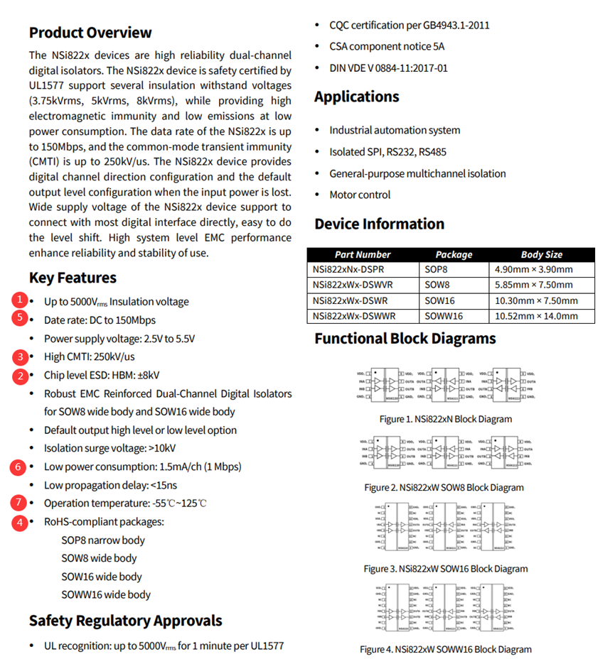
  Although a datasheet lists an array of parameters that may leave you at a loss, such as insulation voltage, CMTI, package, data rate, power consumption, and ESD, Ye identified the items that should be given great attention. Specifically, he listed the following seven key parameters (in no particular order) using NOVOSENSE products as an example.
novosns:Digital isolator selection starts with a good understanding of datasheet

  First, insulation voltage. Isolator is a device that is required to comply with safety regulations, so the isolator selection must be made around safety. Insulation voltage is the most important influencing factor of safety. For example, NOVOSENSE offers a range of basic and enhanced isolators that feature different withstand voltage ranges, so as to meet different system requirements of customers.

  Second, ESD. ESD protection is an important contributor to high reliability of isolator. For the vast majority of chips, ESD immunity is a must-have property, but the capability level requirement depends. Isolators are placed in high-voltage environment, usually the high-low voltage interface in the system, so ESD immunity is also extremely important. NOVOSENSE isolators provide HBM withstand voltage of up to 8kV, the highest chip-level HBM ESD.

  Third, CMTI. It is another key parameter of isolator, which measures a chip’s capability to resist transient interference, that is, the device’s robustness in system applications. CMTI refers to the maximum tolerable rate of short time voltage rise or fall to the value that can destroy the output state of driver. The transient interference is caused by the high DV/DT on the switching node. If the CMTI capability is insufficient, output error or even short circuit may occur, affecting the system safety. The CMTI of isolators from NOVOSENSE is mainly ±200kV/μs, and can even reach ±250kV/μs in some models.

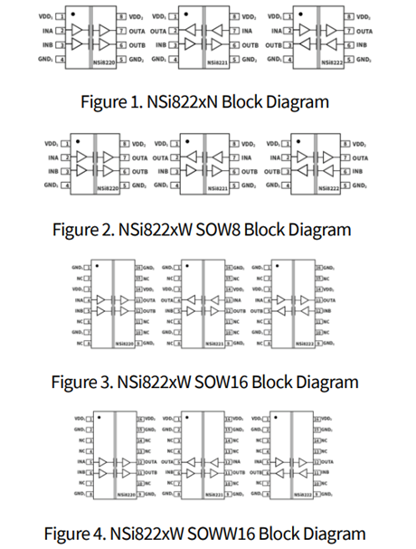
  Fourth, package. Package here is more than body size, and is also related to such parameters as withstand voltage and safe creepage. Different chips will be provided depending on customer requirements or system requirements, but the ultimate objective must be meeting the safety requirements in a smaller and higher-integration package. For example, NOVOSENSE provides different package types including SOP, SOW and SOWW to answer different safety requirements, which will be elaborated later.

  Fifth, data rate and propagation delay. Data rate is an indicator of whether a digital isolator is high-performance, which can be up to hundreds of Mbps or even Gbps level. Different communication standards and interfaces have different requirements for data rate, which need to be carefully checked. However, Ye also underlined that data rate, be it 1Mbps or 150Mbps, has small impact on the device cost. That’s why NOVOSENSE does not provide more product categories by data rate. Instead, basically all digital isolators from NOVOSENSE provide a data rate of 150Mbps, which can meet the requirements of the majority of applications. In addition to data rate, there will also be detailed parameters related to timing in the datasheet, which should also be taken into consideration in the system design.

  Sixth, power consumption. According to Ye, the power consumption of digital isolators has been greatly reduced, relative to optocouplers. Therefore, the power consumption requirement is relatively small, but the datasheet will still describe the power consumption level under various conditions.

  Seventh, operating temperature. Operating temperature is strongly linked to applications. For example, there are four grades of automotive digital isolators, from Grade 0 to Grade 3, which pose different operating temperature requirements. A Grade 0 device is required to cover the temperature range of -40°C-150°C. Industrial digital isolators have different temperature requirements depending on applications, and the maximum requirement is typically -40°C-150°C. These are described in detail in the datasheet.

  How can package make a difference

  As stressed by Ye, package can make a very big difference for isolators. The main reason is that the package size can directly affect the withstand voltage capability of a device. Therefore, particular attention needs to be paid to package. All desire compact devices, but the realization of higher isolation voltage requires a wider-body package. NOVOSENSE has introduced regular package, wide-body package, and ultra-wide-body package. The advantages of ultra-wide-body package are mainly reflected in two parameters – creepage of 15mm, and isolated withstand voltage of 8 kVRMS. Enhanced isolators can provide an insulation level comparable to two basic isolators connected in series. This makes enhanced isolator a perfect choice for some special applications, for example, photovoltaic inverter.
novosns:Digital isolator selection starts with a good understanding of datasheet

  In short, a larger package will allow higher isolation voltage specifications. If you can choose a smaller package to meet the regulatory requirements for the system, the smaller package undoubtedly helps reduce the footprint on board and costs. In addition, you need to consider how many isolation channels the communication interface requires, because the higher the number of channels is, the more important the package type will be.

  Clearance and creepage are two different parameters. Clearance is the shortest spatial distance measured between two conductive parts or between a conductive part and the device interface. Creepage refers to the shortest distance between two conductive parts or between a conductive part and the device interface measured along the insulating surface.

  Clearance and creepage can be affected by environmental pollution level, altitude, and CTI. Particularly in solar and wind power and other continuously operating applications in harsh field conditions, altitude and pollution have a very high impact on clearance and creepage. How can the clearance and creepage requirements be met while reducing the overall size? The CTI of NOVOSENSE products reaches 600V, which can minimize the creepage requirements of the system, thus reducing the system size.

  Safety standards are crucial

  Meeting the parameter specifications alone does not mean the end of isolator selection, and due attention needs to be paid to safety approvals. Isolator is a safety related device, so safety approvals are often shown in the most visible position. For example, the first page of a NOVOSENSE datasheet gives the safety approvals of the device, including UL1577, CQC, CSA and VDE. The reason why certification standards matter greatly is that manufacturers can easily obtain the system safety approvals, provided that they select products that have won safety certification, so that their systems can be used and sold worldwide with great confidence.

  UL1577 standard is a key component level certification requirement for digital isolators, and is applicable to optocouplers, magnetic isolators and capacitive isolators. To obtain the UL1577 approval, a device must withstand the isolation voltage VISO (specified by the manufacturer, usually 2.5kVRMS or 5kVRMS) for 1 minute. The standard also provides that isolators are required to pass 100% production tests using 120% isolation voltage for 1 second.

  In addition, digital isolators also need to refer to regional safety certification standards, such as CQC, CSA, and VDE. Behind the safety approvals are strict test procedures. A device is required to pass aging test, high withstand voltage test, sampling test, extended temperature test, life test and others. It’s especially noted that a complete cycle of life test lasts more than half a year.

  Passing certification tests of agencies does not mean a once-and-for-all thing. When a device is put into mass production, each product needs to be tested. For example, each isolator from NOVOSENSE has passed high voltage test at the factory, and batch sampling tests are carried out on quarterly basis. The complete testing procedures help ensure the safety and reliability of isolators.

  Closing remarks

  The following sections of a datasheet basically include specific pin layout diagrams, property parameters, description of details, detailed measured results, application note, package size diagram, and certification guide, providing references for engineers in different stages of system design.

  Since isolators are not master chips, there are not many do’s and don’ts in their service. For products like main processor, their datasheet may have hundreds of pages. As isolator is safety critical, engineers need to read all the relevant information carefully and fully.

  In the analysis of the datasheet from NOVOSENSE, we have understood how important the key parameters of digital isolator are in product selection, and have got a basic knowledge of safety standards. We also have seen the obvious progresses of devices from NOVOSENSE and Chinese chip makers at large. This is attributable to NOVOSENSE’s ongoing R&D investment, and its product development approach of getting close to applications and market requirements.

  In a nutshell, if you want to use a product or technology well, the first step is to understand it, and the best way to do so is to read its datasheet.

(备注:文章来源于网络,信息仅供参考,不代表本网站观点,如有侵权请联系删除!)

在线留言询价

相关阅读
NSM211x Series High-Precision AEC-Q100 Current Sensors Eliminate Need for External Isolation Components
  NOVOSENSE Microelectronics, a semiconductor company specializing in high-performance analog and mixed-signal chips, has announced the NSM211x, a series of automotive-grade fully integrated high-bandwidth, high-isolation current sensors that both ensure precise current measurement and eliminate the need for any external isolation components.  On display at Electronica 2024 (Stand B5.450), the automotive-grade series targets applications including OBC/DC-DC converters, PTCs, automotive motor control, charging station current detection and fuel cell systems.  Certified to meet AEC-Q100 Grade 0 reliability standards, the series is designed to operate stably within a wide temperature range (-40 to 150°C) and addresses the needs of AC or DC current detection in automotive applications with a high isolation voltage, strong current handling capability and high reliability.  With a -3 dB bandwidth of up to 1 MHz and a response time of 400 ns, the NSM211x series helps control systems achieve rapid loop control and overcurrent protection. The series also features a creepage distance of up to 8.2mm and isolation voltage withstand of 5,000 Vrms per UL standards, with a maximum working isolation voltage of 1,618 Vpk.  It is available in three packaging options, SOP8, SOW16 and SOW10. These respectively have a primary side impedance of 1.2 mΩ, 0.85 mΩ/1 mΩ and an industry leading 0.27mΩ, with a continuous current handling capability of up to 100 A. Multiple product models are available for each package.  The current sensors integrate internal temperature compensation algorithms and offline calibration to enable a high measurement accuracy (<±2% sensitivity error and <±10 mV offset error) across the full temperature range, with no need for secondary programming.  The NSM211x series supports 3.3 V and 5 V power supply voltage as well as DC or AC current measurement with a current range of 5~200 A with options for reference voltage output, overcurrent protection output, and configurable overcurrent protection thresholds.
2024-11-15 14:30 阅读量:365
400mA, High Output Slew Rate: NOVOSENSE's NSOPA240x Series Cracks the Challenge of Resolvers
  With the continuous pursuit of high-precision, high-performance motor control technology, the ability of resolvers, as one of its core components, to accurately measure angular position and rotational speed becomes particularly important.  However, the special requirements of resolver drive circuits have always been a technical bottleneck in the development of the industry. To address this challenge, NOVOSENSE recently released the new NSOPA240x series of operational amplifier, which is designed to simplify circuit design and improve system robustness, bringing innovative solutions to resolver drive applications.  As electromagnetic sensors that can be used to accurately measure angular position and rotational speed, resolvers are widely used in industrial motor controls, servos, robots, and powertrain units in electric and hybrid vehicles. Particularly in electric vehicles, resolvers provide motor control algorithms with precise and stable position information, which is critical to ensuring ideal performance in a wide range of driving conditions. Through their unique operating principle, resolvers provide real-time and accurate feedback on the rotor angle and speed, enabling electric vehicles' motor control algorithms to accurately adjust the current output for smooth driving and instant response. In addition, resolvers' high temperature resistance, simple and reliable mechanism, compact size and low cost make them adaptable to the compact design requirements of electric vehicles and reduce overall costs.  In practice, the design of resolver drive circuits faces multiple challenges. First, the requirements for high current output and high slew rate must be met to ensure a stable excitation signal for resolvers. Second, simplifying circuit design and improving system robustness are also important issues faced by engineers. In addition, complex noise environments and stringent safety requirements bring more difficulties to the design.  With their excellent high gain bandwidth and slew rate, as well as continuous high output current drive function, NOVOSENSE's NSOPA240x high-current output operational amplifiers meet the stringent requirements of resolver primary coils for low-distortion and differential high-amplitude excitation. More importantly, NSOPA240x integrates internal thermal shutdown and overcurrent production, which not only optimizes the circuit design and reduces the system cost, but also significantly improves the overall system reliability and performance.  The automotive version of the NSOPA240x series meets the reliability requirements of AEC-Q100 Grade 1 and can work in harsh environments of -40~125°C. Different channel versions are available to meet different customer needs, with TO252-5 package for single-channel and HTSSOP14 package for dual-channel, as shown in the table below.  High current output capability - adapt to various resolver primary coil drives  Output current capability and output swing are among the most important indicators to measure the driving capability of power amplifiers. The relationship between load current and output swing directly determines the dissipated power in driving operational amplifiers. The excitation primary coil of a resolver usually has a very low DCR (DC resistance), typically less than 100Ω, so a strong current output capability up to 200mA is required to drive the coil. NSOPA240x is designed with a maximum continuous output current capability of 400mA, fully meeting the drive requirements of various resolvers.  High output slew rate - ensure undistorted primary coil excitation signal  Slew rate is one of the most important performance indicators reflecting the dynamic response of an operational amplifier, and the minimum requirement for undistorted sinusoidal signals is shown in the following formula:  Different types of resolvers have different requirements for the amplitude and frequency of the excitation signal. Taking a 7Vrms, 10kHz excitation signal as an example. According to the calculation results of the above formula, the minimum slew rate required to ensure no distortion is about 0.6 V/μs. With a slew rate of 5.5 V/μs, NSOPA240x meets most application requirements for resolver drives.  Integrated current limiting protection and overheating protection - improve resolver system reliability, and reduce complexity and cost  For the power level of several hundred mA at the primary drive end of a resolver, perfect protection measures must be taken, otherwise the system will be seriously threatened or even burned due to overheating and other reasons. NSOPA240x integrates a thermal shutdown protection function. When the chip junction temperature exceeds 173°C, the device will be disabled and the occurrence of a thermal shutdown event will be indicated by the OTF/SH_DN status. To prevent repeated triggering, the overtemperature shutdown function has a temperature hysteresis, where the junction temperature needs to fall back to 155°C before the device is re-enabled and the state of the OTF/SH_DN pin changes to indicate that the thermal shutdown event has stopped.  As shown in the figure below, NSOPA240x can provide customers with system-level functional safety and simultaneously indicate short circuit to power and short circuit to ground.  In addition, each operational amplifier in the chip has current limiting protection for the PMOS (high side) and NMOS (low side) output transistors, because overcurrent may be found on the high side or the low side. And two dedicated pins (as shown in the red box in the figure) are provided to distinguish between high side overcurrent and low side overcurrent, corresponding to the applications of short circuit to ground and short circuit to supply voltage respectively. When the output current returns to normal, the indicator pins will be released synchronously, allowing the system to easily cope with short circuit test scenarios similar to those specified in the ISO 16750 standard.
2024-07-01 13:47 阅读量:309
novosns:Technical Sharing | The Introduction of Gate Drivers and the Applications
  1) Introduction of the Gate Drivers  Gate driver is a buffer circuit between the low-voltage controller and the high-power circuit, which is used to amplify the control signals of the controller for more effective turn-on and turn-off of power devices.  1. The functions of gate driver are as follows  - Gate driver can convert the low-voltage signal from the controller to higher-voltage drive signal, so as to achieve stable turn-on and turn-off of power devices.  - Gate driver can provide transient source and sink peak currents, which can improve the switching speed of power devices and reduce the switching loss.  - Gate driver can effectively isolate the noise of high-power circuits and protect sensitive circuits against interference.  - Gate driver typically integrates protection functions to effectively prevent damages to power devices.  It can be seen that gate driver is used to ensure better performance of power devices in the system.  2. There are four types of common power devices  - Si-MOSFET devices, which withstand voltage of 20V-650V and are suitable for low-power systems.  - Si-IGBT devices, which withstand voltage of greater than 650V and provide a strong current endurance capability. This type is suitable for high-voltage and high-power systems.  --- Both Si-MOSFET and Si-IGBT are Si-based power devices that have been widely used, and their manufacturing technologies are mature and stable.  - SiC-MOSFET devices, which provide withstand voltage range comparable to IGBT, but feature fast switching speed and low switching loss. They are more suitable for high-voltage and high-power systems.  - GaN devices, currently constrained by the manufacturing technology, typically have a withstand voltage of less than 650V, but provide obviously advantageous switching performance. This power device type is suitable for high-frequency and high-power systems.  --- SiC-MOSFET and GaN devices are wide bandgap semiconductors that boast significant performance advantages over Si-based ones, and will have a broad range of applications in the future.  3. NOVOSENSE gate drivers  Different power devices have varied requirements for gate drivers. Currently, NOVOSENSE has developed driver products suitable for these four types of power devices.  4. Switching process of power devices  How does a gate driver control the turn-on and turn-off of power devices? Below is a detailed explanation of the switching process of power devices. In power devices, there are equivalent parasitic capacitances, such as CGS, CGD and CDS. The switching process of a power device can be equivalent to the charging and discharging process of its parasitic capacitances.  4.1 Turn-on process  In the turn-on process, the driver IC connects the output signal to the driver power supply through an internal source current MOS, and charges CGS and discharges CGD through a gate resistor.  - (t0-t1) stage: The gate current charges CGS, and VGS gradually increases. At this point, the power device is still turned off.  - (t1-t2) stage: When VGS increases to a value greater than the gate threshold voltage Vth, the power device begins to turn on, and IDS increases with VGS until it reaches the maximum value.  - (t2-t3) stage: This is the Miller Plateau period, where the gate current mainly discharges CGD, and VDS begins to decrease. The device is fully turned on.  - (t3-t4) stage: The gate current continues to charge CGS, and VGS gradually increases to the power supply voltage. When the gate current reduces to zero, the turn-on process ends. The turn-on loss of the power device mainly occurs at the t1-t3 stage.  4.2 Turn-off process  In the turn-off process, the driver IC connects the output signal to the GND through an internal sink current MOS, and discharges CGS and charges CGD through a gate resistor.  - (t0-t1) stage: The gate current mainly discharges CGS, and VGS gradually decreases.  - (t1-t2) stage: This is the Miller Plateau period, where the gate current mainly charges CGD, and VDS begins to increase. When the voltage reaches VDC, the Miller Plateau ends.  - (t2-t3) stage: IDS begins to decrease. When VGS decreases to Vth, IDS drops to zero, and the power device is completely turned off.  - (t3-t4) stage: The gate current continues to discharge CGS, and VGS eventually drops to zero. The turn-off process ends. The turn-off loss of the power device mainly occurs at the t1-t3 stage.  It can be seen from the analysis above that shortening the t1-t3 stage can effectively reduce the switching loss of power devices.  4.3 Three types of common driver IC  At present, there are three types of commonly used driver ICs, namely non-isolated low-side drivers, non-isolated half-bridge drivers, and isolated drivers.  - Non-isolated low-side drivers are only suitable for power devices with a reference to GND, and provide dual-channel or single-channel driving capability. Non-isolated drivers are relatively simple to implement, requiring only single power supply. They are mainly used in low-voltage systems, such as AC/DC converters, electric tools, and low-voltage DC/DC converters. Currently, NOVOSENSE offers non-isolated low-side driver ICs including NSD1026V and NSD1015.  - Non-isolated half-bridge drivers are used in power systems with a half-bridge configuration. The withstand voltage of the high and low sides is usually achieved through level shifting or isolation, ranging from 200V to 600V. To prevent shoot-through, half-bridge drivers provide an interlock function. When a non-isolated half-bridge driver is used in a system, single power supply plus bootstrap power is typically adopted. This driver IC type is mainly used in low-voltage or high-voltage systems, such as AC/DC converters, motor drives, and on-board DC/DC converters. Currently, the half-bridge driver ICs from NOVOSENSE include NSD1624 and NSD1224.  - Isolated drivers use an internal isolation barrier to physically isolate high and low voltages. Isolated drivers provide flexibility in application. Single-channel and dual-channel isolated drivers are available for low-side, high-side, or half-bridge applications. To achieve primary and secondary isolation in the system, the high-voltage side requires an isolated power supply, making the power supply system relatively complex. Isolated drivers are mainly used in high-voltage systems, such as electric drives, photovoltaic inverters, and OBCs. Currently, NOVOSENSE offers NSI6602 dual-channel isolated driver IC, NSI6601/NSI6601M single-channel isolated driver IC, NSI6801 opto-compatible isolated single-channel driver IC, and NSI6611/NSI68515 smart isolated driver IC.  2) Introduction to Isolation Solutions  In a high-voltage power system, there is usually isolation between high voltage and high voltage, as well as between high voltage and low voltage. Why is isolation driver needed? First, an isolated driver can avoid harm to human body caused by high-voltage electricity, and meet safety standards through isolation. Second, it can protect the control system from damages that can be caused by lightning strikes and high voltage transients. Third, an isolated driver can eliminate ground loops and reduce interference from the high voltage side to the low voltage side. Fourth, it can realize voltage or current change and energy transfer.  There are three commonly used isolation schemes. The first is optocoupler isolation, which achieves signal transmission through light-emitting diodes and phototransistors. This isolation scheme is low-cost, but provides weak CMTI (Common Mode Transient Immunity), limited temperature range, and short service life. The second isolation scheme is magnetic isolation, where the chip integrates micro-transformer and electronic circuit to achieve signal transmission. The magnetic isolation chips deliver benefits such as long lifetime, wide temperature range, and strong CMTI, but involve complex technology, high cost, and prominent EMI issue. The third isolation scheme is capacitive isolation, which achieves signal transmission through isolation capacitors and electronic circuits. It usually uses silicon dioxide (SiO2) as the insulating material. The capacitive isolation scheme features low cost, long isolation life, wide temperature range, and strong CMTI. NOVOSENSE adopts the capacitive isolation scheme.  NOVOSENSE isolation solution  Isolated driver ICs from NOVOSENSE usually have two dies – the primary die on the input side and the secondary die on the output side. There is a physical isolation between the dies. Two isolation capacitors are connected in series on the die to achieve double insulation capability. If one of the dies experiences an EOS failure, the driver IC can still maintain basic insulation capability. The top and bottom substrates of the two isolation capacitors are insulated using SiO2, which can ensure stable material properties, good chip consistency, and long isolation life. The top substrates of the two isolation capacitors are connected by metal wires for signal transmission. NOVOSENSE’s isolated driver ICs can withstand surge voltage up to 12kV and 8kV transient insulation voltage test, far exceeding the insulation requirements of high-voltage systems.  The communication between the dies adopts the differential OOK modulation scheme, which ensures stable and reliable communication. The input signal is modulated at a high frequency and then transmitted from the primary die to the high-voltage die through the isolation capacitor, with the modulation frequency at a level of over 100 MHz. A proprietary CMTI modular circuit is added at the input side of the differential signal, allowing the IC to achieve a stronger CMTI capability up to 150V/ns. For power systems with a high dv/dt, the IC can still work stably without abnormal wave emission.
2024-06-21 11:23 阅读量:553
On the Fast Lane: NOVOSENSE's Ongoing Commitment to Automotive Chip Excellence
  Automobiles are undergoing increasing electrification and digitalization, from electric drive trains to immersive infotainment systems in the cockpit.  NOVOSENSE, a pioneering force in the automotive chips, recently unveiled several groundbreaking products aimed at enhancing performance, reliability, and efficiency in automotive applications.  NCA1462-Q1, an automotive-qualified CAN SIC based on innovative ringing suppression patent  NCA1462-Q1 is based on its proprietary innovative ringing suppression patent. Compared with CAN FD solution, NCA1462-Q1 is further compatible with the CiA 601-4 standard on the premise of meeting the ISO 11898-2:2016 standard, and can achieve a data rate of ≥8Mbps. With NOVOSENSE's patented ringing suppression function, NCA1462-Q1 maintains good signal quality even in the case of star network multi-node connection; in addition, its ultra-high EMC performance and more flexible VIO as low as 1.8V can effectively help engineers simplify system design and create high-quality automotive communication system.  NSHT30-Q1, a relative humidity (RH) and temperature sensor based on CMOS-MEMS  NSHT30-Q1 integrates a complete sensor system on a single chip, including a capacitive RH sensor, CMOS temperature sensor and signal processor, and an I2C digital communication interface. It is designed in DFN package with Wettable Flank, and the product size is 2.5mm×2.5mm×0.9mm. NSHT30-Q1's I2C interface features two selectable addresses with communication speed up to 1 MHz and supports a wide supply voltage range of 2.0V~5.5V.  NSOPA9xxx series, general-purpose operational amplifiers for automotive applications  NSOPA9xxx series is suitable for 40V high voltage and offers a variety of product models with bandwidth option of 1MHz/5MHz/10MHz and 1/2/4-channel. It meets the reliability requirements of AEC-Q100 Grade 1, and can operate from -40°C to 125°C. Different package versions are available to meet different customer needs: SOT23-5, SOP-8 for 1-channel; MSOP-8, SOP-8 for 2-channel; and TSSOP-14, SOP-14 for 4-channel.  NSD3604/8-Q1, a new automotive-qualified 4/8-channel multi-channel half-bridge driver  NSD3604/8-Q1 can drive multiple loads and is used in automotive domain control architecture. It covers 4/8-channel half-bridge drive which can drive 4 DC brushed motors, and achieve multi-channel high-current motor drive, and also be used as a multi-channel high-side switch drive. NSD3604/8-Q1 is suitable for multi-motor or multi-load applications, such as car window lifting, electric seats, door locks, electric tailgates, and proportional valves and other body control applications.
2024-04-17 13:24 阅读量:588
  • 一周热料
  • 紧缺物料秒杀
型号 品牌 询价
MC33074DR2G onsemi
CDZVT2R20B ROHM Semiconductor
RB751G-40T2R ROHM Semiconductor
TL431ACLPR Texas Instruments
BD71847AMWV-E2 ROHM Semiconductor
型号 品牌 抢购
TPS63050YFFR Texas Instruments
IPZ40N04S5L4R8ATMA1 Infineon Technologies
STM32F429IGT6 STMicroelectronics
ESR03EZPJ151 ROHM Semiconductor
BP3621 ROHM Semiconductor
BU33JA2MNVX-CTL ROHM Semiconductor
热门标签
ROHM
Aavid
Averlogic
开发板
SUSUMU
NXP
PCB
传感器
半导体
相关百科
关于我们
AMEYA360微信服务号 AMEYA360微信服务号
AMEYA360商城(www.ameya360.com)上线于2011年,现 有超过3500家优质供应商,收录600万种产品型号数据,100 多万种元器件库存可供选购,产品覆盖MCU+存储器+电源芯 片+IGBT+MOS管+运放+射频蓝牙+传感器+电阻电容电感+ 连接器等多个领域,平台主营业务涵盖电子元器件现货销售、 BOM配单及提供产品配套资料等,为广大客户提供一站式购 销服务。