- Ameya360 Component Supply Platform >
- Trade news >
- Intense Competition in Advancing Processes at the 2nm by Samsung, Intel, and TSMC
Intense Competition in Advancing Processes at the 2nm by Samsung, Intel, and TSMC
According to TechNews’ report, Gitae Jeong, Vice President of Samsung Electronics, recently revealed in an interview that the company is set to introduce the SF1.4 (1.4nm) process, expected to enter mass production in 2027.

This announcement intensifies the competition in advanced semiconductor manufacturing, particularly in the development of 2.5D/3D integrated heterogeneous structure packaging among the three major semiconductor foundry giants.
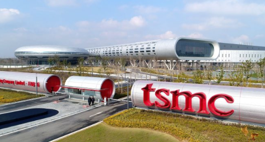
*TSMC: N3P Process Superior to Intel 18A, N2 to Lead Industry’s Advanced Processes
Previously, the semiconductor industry reported challenges with both TSMC and Samsung achieving yields above 60% for their 3nm processes due to undisclosed issues. TSMC’s yield was reported to be only 55%, below the normal yield rate.
However, TSMC’s President, C.C. Wei, expressed optimism, stating that current N3 demand is better than three months ago, contributing to a healthy growth outlook for TSMC in 2024.
Wei also anticipates that TSMC’s 3nm process will contribute a mid-single-digit percentage (4%-6%) to the company’s annual wafer revenue in 2023.
Regarding competition with rival Intel’s 18A process, Wei believes that TSMC’s N3P process offers better performance, power, and area (PPA), alongside improved cost efficiency and technical maturity. Furthermore, TSMC’s upcoming N2 process is expected to be the industry’s most advanced when introduced.
*Intel: Striving for the Fourth Customer for 18A Process Outsourcing Orders
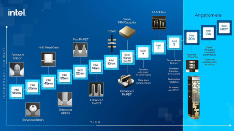
Intel’s CEO, Pat Gelsinger, has revealed that the 18A process has secured orders from three customers and aims to acquire a fourth customer by the end of the year. The advanced 18A process is scheduled to begin production at the end of 2024, with one customer already having made an advance payment. External expectations suggest that the customer could possibly be NVIDIA or Qualcomm.
Intel has stated that Intel 4 and Intel 3 processes are similar, as are Intel 20A and Intel 18A processes. Consequently, Intel’s primary focus will be on offering Intel 3 and Intel 18A to semiconductor foundry customers. Meanwhile, Intel 4 and Intel 20A processes are more likely to be used internally. However, Intel is open to accommodating customer requests if they express interest in adopting these later processes.
*Samsung: Commencing Mass Production of SF2 in 2025, Prioritizing Internal Use
Due to challenges with the three-nanometer (3nm) manufacturing process, there have been reports that Samsung plans to shift directly to the more advanced two-nanometer (2nm) process.
According to Samsung’s Foundry Forum (SFF) plan, they will begin mass production of the 2nm process (SF2) in 2025 for mobile applications, expand to high-performance computing (HPC) applications in 2026, and further extend to the automotive sector and the expected 1.4nm process by 2027.
Similar to Intel, Samsung intends to prioritize the production of its own products using the 2nm process. The 2nm process products will initially be utilized for Samsung’s in-house products rather than external customer products.
*Summary
While TSMC’s N3 series currently enjoys broad support, including N3E, N3X, and N3P process series, the move to 2nm introduces new variables as it adopts a completely new GAAFET architecture. Regardless, whether it’s TSMC’s N2, Intel’s 18A, or Samsung’s SF2, each of them possesses its competitive strengths. The industry is also eagerly anticipating the future developments in advanced semiconductor processes.
Online messageinquiry
TSMC Expected to Lower Capital Expenditure, Potentially Falling Below $30 Billion for the Year
- Week of hot material
- Material in short supply seckilling
| model | brand | Quote |
|---|---|---|
| CDZVT2R20B | ROHM Semiconductor | |
| MC33074DR2G | onsemi | |
| RB751G-40T2R | ROHM Semiconductor | |
| BD71847AMWV-E2 | ROHM Semiconductor | |
| TL431ACLPR | Texas Instruments |
| model | brand | To snap up |
|---|---|---|
| ESR03EZPJ151 | ROHM Semiconductor | |
| BP3621 | ROHM Semiconductor | |
| STM32F429IGT6 | STMicroelectronics | |
| TPS63050YFFR | Texas Instruments | |
| IPZ40N04S5L4R8ATMA1 | Infineon Technologies | |
| BU33JA2MNVX-CTL | ROHM Semiconductor |
- Week of ranking
- Month ranking
Qr code of ameya360 official account
Identify TWO-DIMENSIONAL code, you can pay attention to


Please enter the verification code in the image below:
