Aluminum-based PCB vs Ceramic-based PCB – A Comprehensive Comparison for Your Electronics

发布时间:2023-12-15 13:26
作者:AMEYA360
来源:网络
阅读量:1701

  In the realm of electronics, the choice of printed circuit board (PCB) material plays a pivotal role in determining the functionality, performance, and longevity of electronic devices. Two prominent contenders in this domain are aluminum-based PCBs and ceramic-based PCBs, each with its distinct advantages and specialized applications. Let’s delve deeper into the characteristics, pros, and cons of aluminum-based PCB vs ceramic-based PCB to aid in your decision-making process.
Aluminum-based PCB vs Ceramic-based PCB – A Comprehensive Comparison for Your Electronics

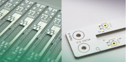
  Aluminum-based PCBsAluminum-based PCBs, also recognized as metal core PCBs (MCPCBs), boast a core constructed from an aluminum alloy. These boards have garnered attention for their exceptional thermal conductivity and find extensive usage in applications that demand efficient heat dissipation.

  Aluminum-based PCBs

  Advantages of Aluminum-based PCBs

  Thermal Conductivity: The standout feature of Aluminum-based PCBs is their remarkable thermal conductivity. This property makes them a preferred choice in applications where heat dissipation is critical, such as LED lighting systems, power converters, and automotive electronics. The ability to efficiently transfer heat away from sensitive components ensures enhanced reliability and longevity of the devices.

  Cost-Efficiency: Aluminum-based PCBs often present a more budget-friendly option compared to certain high-performance materials. This cost-effectiveness makes them attractive for projects where optimizing expenses without compromising quality is a priority.

  Lightweight Nature: Despite their robust construction, Aluminum-based PCBs maintain a relatively lightweight profile. This attribute proves advantageous in applications where weight considerations are pivotal, such as portable electronic devices or aerospace applications.

  Manufacturing Simplicity: The manufacturing process for Aluminum-based PCBs is often simpler and more straightforward compared to some other materials, leading to reduced production time and costs.

  However, these PCBs do come with their set of limitations, which might impact their suitability for specific applications.

  Limitations of Aluminum-based PCBs

  Electrical Insulation Requirements: Aluminum-based PCBs necessitate an insulating layer between the circuit and the metal base to prevent short circuits. This requirement adds complexity to the manufacturing process and design considerations, potentially increasing production costs.

  Mechanical Strength: While durable, Aluminum-based PCBs might not offer the same level of mechanical strength as Ceramic-based PCBs. This factor could limit their use in applications exposed to harsh physical environments or substantial mechanical stress.

  Ceramic-based PCBsCeramic-based PCBs, typically crafted from materials like aluminum oxide or aluminum nitride, have gained prominence owing to their outstanding electrical insulation properties and reliability in diverse applications.

  Ceramic-based PCBs

  Advantages of Ceramic-based PCBs

  Superior Electrical Insulation: The hallmark of Ceramic-based PCBs lies in their superior electrical insulation capabilities. These boards excel in preventing signal interference and short circuits, making them ideal for high-voltage applications where maintaining signal integrity is crucial.

  Enhanced Mechanical Strength: Ceramic-based PCBs exhibit greater mechanical strength compared to their Aluminum-based counterparts. This characteristic makes them well-suited for deployment in rugged environments or applications where resistance to mechanical stress is imperative.

  High-Frequency Applications: With low dielectric loss and excellent signal integrity properties, Ceramic-based PCBs are highly sought after for high-frequency circuits and radio frequency (RF) applications.

  Chemical Resistance: Ceramics demonstrate remarkable resistance to chemicals and corrosion, making Ceramic-based PCBs suitable for applications exposed to harsh and corrosive environments, such as in aerospace or industrial settings.

  However, these boards also come with certain limitations that might influence their suitability for specific projects.

  Limitations of Ceramic-based PCBs

  Cost Considerations: Ceramic-based PCBs typically entail higher manufacturing costs due to the expense of materials and the complexity involved in their production. This factor might limit their feasibility for projects with stringent budget constraints.

  Brittleness: Despite their mechanical strength, ceramics can be inherently brittle. Careful handling is required during production, assembly, and installation to prevent breakage, which can add to the overall project timeline and costs.

  ConclusionThe choice between Aluminum-based and Ceramic-based PCBs hinges on a comprehensive evaluation of your project’s requirements, budget considerations, and the specific environmental conditions the electronic device will encounter.

  For applications where thermal management and cost-effectiveness are paramount, Aluminum-based PCBs might prove more suitable. Conversely, if superior electrical insulation, mechanical robustness, and reliability in harsh conditions are essential, Ceramic-based PCBs could be the preferred option.

  Ultimately, consulting with experienced PCB manufacturers or engineers remains pivotal in making an informed decision aligned with the unique demands of your electronic project.

(备注:文章来源于网络,信息仅供参考,不代表本网站观点,如有侵权请联系删除!)

在线留言询价

相关阅读
Introduction to PCB Manufacturing Machines : Types
  In the ever-evolving world of electronics, Printed Circuit Boards (PCBs) are the unsung heroes that form the backbone of most electronic devices. From smartphones to industrial machinery, PCBs provide the essential connections between various components, ensuring that signals are transmitted effectively and reliably. As demand for electronic devices continues to surge, the need for efficient, high-quality PCB manufacturing has never been greater. This is where PCB manufacturing machines come into play.  These machines are pivotal in the production process, transforming raw materials into complex circuit boards that meet stringent specifications. In this introduction, we will explore the different types of PCB manufacturing machines and highlight some of the key players in the industry.  Types of PCB Manufacturing Machines  1. PCB Fabrication MachinesPCB fabrication is the process of creating the physical circuit board from a design. This involves several key steps, each facilitated by specific types of machines:  – Photoplotters: These are used to create photomasks for PCB production. A photomask is a plate with patterns that will be transferred onto the PCB’s surface. Photoplotters use high-precision imaging technology to ensure accurate pattern reproduction.  – Drilling Machines: Once the PCB pattern is applied, drilling machines create holes for components and vias. These machines are equipped with high-speed spindles and precision control systems to ensure that holes are drilled accurately and efficiently.  – Etching Machines: After drilling, the PCB is subjected to an etching process to remove unwanted copper and leave behind the circuit pattern. Etching machines use chemical solutions or abrasive materials to strip away excess copper while preserving the desired circuitry.  – Laminators: Laminating machines are used to bond multiple layers of PCBs together. This process involves applying heat and pressure to laminate the layers into a single, multi-layer board. Laminators ensure that the layers are aligned correctly and that the adhesive bonds are strong.  – Solder Mask and Silkscreen Printers: Solder masks are applied to prevent solder from bridging between circuit paths, while silkscreen printers add labels and markings to the PCB. These machines use advanced printing technologies to apply precise coatings and markings.  2. PCB Assembly MachinesOnce the PCB is fabricated, it needs to be assembled with electronic components. This step involves several specialized machines:  – Pick and Place Machines: These are crucial for the assembly process. Pick and place machines automatically position and place components onto the PCB. They use high-speed cameras and advanced algorithms to ensure components are placed accurately and efficiently.  – Soldering Machines: There are various types of soldering machines used in PCB assembly. Wave soldering machines apply solder to the entire PCB at once, while reflow soldering machines use heat to melt solder paste and create precise solder joints. Selective soldering machines target specific areas for soldering, reducing the risk of damage to sensitive components.  – Inspection Machines: Quality control is essential in PCB manufacturing. Automated Optical Inspection (AOI) machines use cameras and image processing to detect defects such as soldering errors, missing components, or alignment issues. X-ray inspection machines can inspect internal layers and connections that are not visible externally.  3. PCB Testing MachinesTesting is a crucial step to ensure the functionality and reliability of the PCBs. Testing machines include:  – In-Circuit Testers (ICT): These machines test the electrical connections and functionality of the PCB by probing each point and checking for continuity, shorts, and other electrical faults.  – Functional Testers: Functional testers simulate the PCB’s operating environment to ensure that it performs as expected. These testers are used to evaluate the board’s overall functionality and identify any operational issues.
2025-03-21 13:32 阅读量:201
Difference between Diode and Triode in PCBA manufacturing
  In printed circuit board assembly (PCBA) manufacturing, understanding the differences between diode and triode is crucial for designing efficient electronic circuits. Both components play essential roles in controlling the flow of electrical current, but they have distinct characteristics that determine their specific applications and functionalities.  Diode:Diode  A diode is a two-terminal electronic component that primarily allows current to flow in one direction while blocking it in the opposite direction. Here are key characteristics and uses of diodes in PCBA manufacturing:  1. Functionality: Diodes are used for rectification, converting AC (Alternating Current) to DC (Direct Current). They ensure that current flows in only one direction, preventing reverse polarity which can damage sensitive components.  2. Types: Common types include:  – Rectifier Diodes: Used in power supplies to convert AC to DC.  – Zener Diodes: Maintain a constant voltage for regulation.  – Light-Emitting Diodes (LEDs): Emit light when current flows through them, used for indicators and displays.  3. Applications: Diodes are found in almost all electronic circuits:  – Power supplies  – Signal demodulation  – Overvoltage protection  – Voltage regulation  Triode (Transistor):Triode  A triode, also known as a transistor, is a three-terminal semiconductor device that amplifies or switches electronic signals and electrical power. Here are the key characteristics and uses of triodes in PCBA manufacturing:  1. Functionality: Triodes can amplify current, acting as switches or amplifiers depending on the configuration:  – Bipolar Junction Transistors (BJTs): Amplify current and are used for analog circuits.  – Field-Effect Transistors (FETs): Control current flow with an electric field, used in digital circuits.  2. Types: Different types cater to specific applications:  – NPN and PNP BJTs: Common bipolar transistor types.  – MOSFETs (Metal-Oxide-Semiconductor Field-Effect Transistors): High-speed switching in digital circuits.  – JFETs (Junction Field-Effect Transistors): Used in amplifiers and analog switches.  3. Applications: Triodes are essential in modern electronics:  – Amplifiers in audio systems  – Switching circuits in digital logic gates  – Oscillators in radio frequency applications  – Drivers for motors and relays  Comparison– Function: Diodes primarily control current direction, whereas triodes amplify or switch currents.  – Configuration: Diodes are two-terminal devices, while triodes (transistors) have three terminals: emitter, base, and collector.  – Applications: Diodes are crucial for power supply and signal processing, while triodes are fundamental in amplification and digital switching.  In conclusion, while diodes and triodes are both essential components in PCBA manufacturing, their distinct functionalities and applications make them suitable for different roles within electronic circuits. Understanding their differences is key to designing and assembling efficient and reliable electronic devices.
2024-08-16 14:24 阅读量:445
What is “component placement” in PCB?
  Component placement is a critical step in the PCB assembly process where electronic components are precisely positioned and soldered onto the printed circuit board (PCB). This phase plays a crucial role in ensuring the functionality, reliability, and performance of the final electronic device. Let’s delve into the details of component placement in PCB assembly.  How many electronic components are there?1. Surface Mount Devices (SMDs):  – Passive Components: Resistors, capacitors, inductors.  – Active Components: Integrated circuits (ICs), transistors, diodes.  2. Through-Hole Components:  – Components with leads that pass through holes drilled in the PCB.  What is the component placement process?1. Design for Assembly (DFA)  Before physical assembly begins, the PCB layout and design must consider DFA principles:  – Component Orientation: Optimizing orientation for ease of assembly and efficient routing of traces.  – Clearance and Spacing: Ensuring adequate space for soldering and avoiding interference between components.  – Accessibility: Facilitating automated or manual assembly processes.  2. Automated Component Placement  Modern PCB assembly typically involves automated pick-and-place machines:  – Vision Systems: Cameras identify fiducial markers or component outlines on the PCB to align and place components accurately.  – Component Feeding: Components are loaded into feeders, which supply them to the pick-and-place machine.  – Pick-and-Place Process: The machine picks components from the feeder using vacuum nozzles, aligns them precisely over corresponding pads on the PCB, and places them gently using controlled motion.  3. Manual Component Placement  For specialized components or low-volume production, manual placement may be used:  – Skill and Precision: Technicians use hand tools like tweezers and magnifiers to place components accurately.  – Prototype Builds: Initial prototypes or small batches may benefit from manual placement for flexibility and customization.  What should be considered when placing components in PCB?Component placement is more than just arranging components on a board; it involves strategic decisions that impact the overall functionality and quality of the PCB. Proper placement not only ensures that the circuit operates correctly but also affects signal integrity, thermal management, and ease of assembly. Here are some crucial aspects to consider:  1. Design for Signal Integrity  Signal integrity is crucial for the proper operation of high-speed digital circuits and sensitive analog circuits. To maintain signal integrity:  – Minimize Trace Length: Place critical components closer together to minimize trace lengths, reducing signal delay and electromagnetic interference (EMI).  – Signal Paths: Follow a logical signal flow from input to output, avoiding crossing high-speed signals with noisy or high-current traces.  – Grounding: Ensure a solid ground plane and place components that require low impedance connections to ground strategically to minimize noise and ground loops.  2. Thermal Management  Certain components, such as power transistors or voltage regulators, generate heat during operation. Efficient thermal management is essential to prevent overheating and ensure reliability:  – Heat Sinks: Provide adequate space and mounting locations for heat sinks or thermal pads.  – Airflow: Arrange components to allow natural or forced airflow across heat-generating components.  – Isolation: Keep heat-sensitive components away from those generating significant heat to prevent thermal damage.  3. Manufacturability and Assembly  Designing for manufacturability involves ensuring that the PCB can be efficiently assembled with minimal errors and rework:  – Component Accessibility: Ensure components are placed such that they can be easily soldered by hand or by automated pick-and-place machines.  – Orientation: Align components consistently for ease of assembly and to avoid errors during soldering.  – Clearance and Spacing: Adhere to manufacturing guidelines for minimum clearance between components, ensuring soldering and inspection can be done without issues.  4. Electromagnetic Compatibility (EMC)  PCB layout plays a crucial role in achieving EMC compliance by reducing EMI emissions and susceptibility:  – Component Arrangement: Position sensitive components and traces to minimize loop areas and coupling.  – Shielding: Group and shield sensitive components from noise sources such as high-current paths or switching circuits.  – Grounding and Routing: Properly route and ground signal return paths to reduce loop areas and impedance discontinuities.  Best Practices for Component Placement– Start with Critical Components: Begin by placing critical components such as microcontrollers, connectors, and high-frequency components based on their functional and spatial requirements.  – Use Design Tools: Leverage PCB design software with simulation capabilities to visualize signal paths, analyze thermal performance, and optimize placement before fabrication.  – Iterative Refinement: Iterate the placement based on simulation results, design reviews, and practical considerations to achieve the best balance of performance and manufacturability.  – Documentation: Clearly label components with reference designators and polarity markings on the silkscreen layer. Maintain an updated BOM (Bill of Materials) to ensure accurate procurement and assembly.  ConclusionComponent placement in PCB assembly is a pivotal stage where careful planning, advanced technology, and skilled craftsmanship converge to create reliable electronic devices. By adhering to DFA principles, leveraging automation, and considering thermal and signal integrity factors, manufacturers can achieve efficient, high-quality assembly that meets the demands of today’s electronics industry. As technology advances, component placement continues to evolve, driving innovation and pushing the boundaries of what’s possible in electronic design and manufacturing.
2024-07-18 11:48 阅读量:666
15 Common PCB Circuit Effects
  Printed Circuit Boards (PCBs) are the backbone of modern electronics, serving as the foundation for countless devices we rely on daily. However, designing and working with PCBs come with its own set of challenges and nuances. In this guide, we delve into 15 common circuit effects that engineers and enthusiasts encounter when designing and troubleshooting PCBs.  Each effect explored here sheds light on a specific aspect of PCB design, whether it’s related to signal integrity, power distribution, or electromagnetic interference. Through concise explanations and practical examples, we aim to equip readers with a deeper understanding of these effects, enabling them to optimize their PCB designs for performance, reliability, and manufacturability.  Whether you’re a seasoned electronics engineer or a hobbyist diving into the world of PCB design, this guide is designed to serve as a valuable reference, helping you navigate the intricacies of PCB circuits with confidence and expertise.  1. Drawbridging effectIn high-density wiring, when there is not enough space between two lines, a situation may occur where one line hangs over another line, similar to the shape of a suspension bridge.  The drawbridging effect usually occurs in PCB design, especially in cases where a large number of signal lines need to be arranged and space is limited. The drawbridging effect may lead to problems such as signal crosstalk, electromagnetic interference, signal distortion, or delay.  Measures to reduce the drawbridging effect:  Reasonably plan the PCB layout, try to keep the signal lines arranged in a straight line, and avoid situations where lines cross or overlap.  Optimize PCB routing, try to increase the spacing between signal lines as much as possible to avoid the suspension bridge effect caused by too small spaces.  Use layered PCB design to arrange different signal lines on different layers to reduce crossing and interference between lines.  Reduce electromagnetic interference between signal lines by appropriate signal layer and ground layer planning to improve the circuit’s anti-interference ability.  2. Ripple effectIn high-speed circuits, when the signal transmission speed is fast, the signal may undergo ripple deformation when propagating on the PCB, affecting the signal quality, including signal distortion, clock offset, crosstalk, and interference.  Measures to reduce ripple effects:  Optimize PCB layout and routing to minimize the bending, crossing, and branching of signal lines, and maintain the consistency of signal transmission paths.  Adopt appropriate signal line and ground design to reduce crosstalk and interference between signal lines, improving signal transmission quality.  Use signal compensation or pre-emphasis technology to compensate for and enhance the signal, reducing waveform distortion and deformation.  Choose appropriate signal transmission lines and signal processing devices to improve the circuit’s anti-interference ability and transmission speed.  3. Overshoot effectSudden voltage changes that occur during signal transmission may cause excessive voltage shock to components on the circuit board, damaging components or causing circuit failures.  Overshoot effects may be caused by excessively fast rising or falling edges of the signal, or by the instability of the signal transmission line or signal source.  Measures to reduce overshoot effects:  Optimize the design of signal transmission lines to ensure the impedance matching and stability of the signal lines.  Use appropriate power filters and power decoupling capacitors to reduce interference from signal sources.  Adopt signal pre-emphasis technology or signal compensation technology to preprocess or compensate the signal, reducing the occurrence of overshoot effects.  Choose appropriate components and circuit protection devices to improve the circuit’s resistance to overshoot and stability.  4. Resonance effectParameters such as inductance, capacitance, and impedance on the circuit board may cause resonance of the signal at specific frequencies, affecting the stable transmission of the signal. This resonance phenomenon usually occurs at specific frequencies when the frequency of external signals matches the resonant frequency of the circuit, causing resonance effects.  Measures to reduce resonance effects:  Optimize PCB layout and design to avoid situations where the circuit has a resonant frequency close to the excitation frequency.  Use compensation circuits or filters to eliminate or suppress resonance effects.  Choose appropriate damping components or damping materials to reduce the impact of resonance effects.  Adopt appropriate circuit tuning techniques to stabilize the circuit’s frequency response within a specific frequency range.  5. Floating EffectIn high-speed circuits, due to factors such as electromagnetic radiation, signals may float on the surface of conductors or circuit boards, affecting signal transmission and reception.  To reduce the impact of PCB floating effect on circuits, designers can take the following measures:  Measures to Reduce Floating Effect:  Optimize PCB layout and design, plan the routing and spacing of signal lines reasonably, and minimize the impact of electromagnetic radiation on signal transmission.  Use appropriate signal line and ground line designs to ensure impedance matching and stability of signal lines.  Use shielding covers or shielding materials to reduce electromagnetic radiation and interference.  Select suitable PCB materials and components to reduce the occurrence of floating effects.  6. Crosstalk EffectDue to factors such as dense layout of PCB signal lines or electromagnetic interference, different signal lines may experience crosstalk. Crosstalk can lead to degradation of signal quality or abnormal circuit function.  Measures to Reduce Crosstalk Effect:  Optimize PCB layout and design, plan the routing and spacing of signal lines reasonably, and minimize mutual interference between signal lines.  Use shielding covers, shielding materials, or ground isolation techniques to reduce the impact of electromagnetic interference on signals.  Use differential signal transmission lines or increase signal layers to improve anti-interference capability and reduce the occurrence of crosstalk.  Select suitable PCB materials and components to reduce the impact of crosstalk effects.  7. Reflection EffectRefers to the phenomenon in high-speed signal transmission where signals encounter impedance mismatch or incomplete absorption of signal energy by the terminal of the signal transmission line, resulting in signals reflecting back to the original source end. This reflection effect may cause signal waveform distortion, affecting the transmission quality and stability of the circuit.  Measures to Reduce Reflection Effect:  Design signal transmission lines reasonably to ensure impedance matching and minimize impedance mismatch situations.  Use terminal resistors or terminal capacitors to absorb signal energy and reduce signal reflection.  Optimize PCB layout and design to minimize the length of signal transmission lines and reduce signal transmission delay.  Select suitable PCB materials and components to reduce the impact of reflection effects.  8. Shielding EffectThe metal layer or shielding cover on the PCB may shield signals, affecting the transmission range and quality of signals.  Measures to Reduce Shielding Effect:  Design PCB layout reasonably: Try to avoid overlap or proximity between signal lines and shielding areas to minimize the impact of shielding effect.  Choose appropriate shielding materials: Select suitable metal layers or shielding cover materials in PCB design to have good shielding performance while minimizing the impact on signal transmission.  Design suitable grounding structure: A good grounding structure can help reduce the shielding effect of signals and improve signal transmission quality.  Pay attention to signal adjustment: For signals that need to pass through shielding areas, signal adjustment techniques can be employed to minimize the impact of shielding effect, such as increasing signal power or adjusting signal transmission methods.  9. Thermal Expansion EffectTemperature changes may cause thermal expansion or contraction of PCB materials, affecting the dimensional stability of circuit boards and the connection status of components.  Measures to Reduce Thermal Expansion Effect:  Choose appropriate PCB materials: Selecting PCB materials with smaller coefficients of thermal expansion can reduce the impact of thermal expansion on circuits.  Design PCB layout reasonably: During PCB design, try to avoid direct connection between materials with high coefficients of thermal expansion and those with low coefficients to reduce the impact of thermal expansion.  Control soldering temperature: Control soldering temperature and time during the soldering process to avoid excessive temperature leading to solder joint failure or component displacement.  Use support structures: Adding appropriate support structures in PCB design can reduce PCB bending deformation, improving the stability and reliability of the PCB.  10. Ground Hole EffectThere are many ground holes on the PCB. When ground holes are close to signal lines or other ground holes, ground hole effect may occur, affecting the stability of signal transmission.  Measures to Reduce Ground Hole Effect:  Design ground holes reasonably: Design appropriate parameters for ground holes, such as diameter, pitch, copper foil diameter, etc., to ensure impedance matching and consistency of ground holes, reducing ground hole inductance and crosstalk effects.  Use ground hole filling: Ground hole filling techniques can be employed in PCB design to fill ground holes, reducing their impact on signal transmission and improving PCB performance stability.  Optimize layout: Plan PCB layout reasonably to minimize the number and density of ground holes, reducing their impact on circuits.  Adjust interlayer stacking: Choose PCB layer stacking methods appropriately to minimize ground holes between inner and outer layers, reducing the impact of ground hole effect.  11. Filling EffectThe filling material on the PCB may affect signal transmission. For example, differences in the dielectric constant of the filling material may cause changes in signal transmission speed or signal attenuation.  Measures to Reduce Filling Effect:  Choose filling material reasonably: Select filling materials with a dielectric constant close to that of the PCB material to reduce the impact of dielectric constant differences on signal transmission.  Control the thickness of filling material: Properly control the thickness of filling material to avoid excessive thickness, which could lengthen the signal transmission path and increase attenuation.  Optimize PCB layout: During PCB design, minimize the impact on signal transmission paths, plan filling areas reasonably, and avoid interference from filling materials on signal transmission paths.  Use low-loss filling materials: Choose filling materials with low resistance and dielectric loss to minimize attenuation and distortion during signal transmission.  12. Temperature Drift EffectTemperature changes on the PCB may cause thermal expansion or contraction of circuit board materials, thereby affecting the dimensional stability of the circuit board and the connection status of components.  Measures to Reduce Temperature Drift Effect:  Choose PCB materials reasonably: Select PCB materials with good thermal stability and dimensional stability to reduce the impact of temperature changes on the PCB.  Control soldering temperature: During the soldering process, control soldering temperature and time properly to avoid excessive soldering temperature leading to damage or breakage of components and solder joints.  Optimize PCB layout: Plan PCB layout reasonably to reduce differences in thermal expansion coefficients between components and avoid changes in the connection status of components due to temperature changes.  Temperature environment control: Control temperature changes in the PCB usage environment to avoid significant temperature shocks to the PCB, thereby reducing the impact of temperature changes on PCB circuits.  13. Crystal EffectDevices such as transistors in PCB routing may be influenced by the surrounding environment, causing changes in device parameters and affecting circuit performance.  Measures to Reduce Crystal Effect:  Rational Layout: Properly plan PCB layout to avoid external interference affecting devices such as transistors and minimize electromagnetic field interference with devices.  Temperature Control: Take measures to control the operating temperature of the PCB board during design and manufacturing to reduce the influence of temperature changes on device parameters and improve circuit stability.  Choose Appropriate Devices: Select transistors and other devices with good anti-interference and stability to reduce the impact of crystal effect on the circuit.  Design Compensation Circuits: In PCB design, compensation circuits can be used to correct drift in device parameters, improving circuit performance and stability.  14. Restricted EffectThere are some restricted areas on the PCB, such as edges, power supply areas, etc., which may impose certain limitations or impacts on signal transmission or routing.  Measures to Reduce Restricted Effect:  Rational Planning of Layout: During PCB design, plan the layout reasonably to avoid placing sensitive signal lines or components near restricted areas, reducing the impact of restrictions.  Electromagnetic Shielding: For areas prone to electromagnetic interference in restricted areas, electromagnetic shielding measures can be adopted, such as placing metal shielding covers around sensitive areas to reduce the impact of external electromagnetic interference on the circuit.  Optimization of Power Supply Design: For possible power supply instability or noise issues in power supply areas, measures such as optimizing power supply design, adding filtering circuits, and reducing power supply noise can be taken to improve power supply stability and circuit performance.  Fine Routing: When routing in restricted areas, adopt fine routing methods as much as possible to reduce restrictions or elongation of signal transmission paths, improving signal transmission rate and stability.  15. Landmine EffectHidden problems or faults on PCB boards may suddenly appear during subsequent testing or use, causing unexpected impacts or damage to the circuit board.  Measures to Reduce Landmine Effect:  Strict Quality Control: During PCB production, strictly control the quality of each process to ensure that each component and circuit connection meets specifications, reducing hidden dangers.  Perfect Testing Procedures: Establish comprehensive testing and inspection procedures to conduct comprehensive testing and inspection of PCB circuits, promptly identify and repair potential problems.  Use Reliable Components: Choose components and materials with high reliability and stable quality to reduce the probability of failure and minimize the occurrence of landmine effects.  Strengthen Maintenance: Regularly maintain and upkeep produced PCB circuits, promptly identify and repair potential problems, improving circuit reliability and stability.
2024-04-30 10:11 阅读量:528
  • 一周热料
  • 紧缺物料秒杀
型号 品牌 询价
BD71847AMWV-E2 ROHM Semiconductor
CDZVT2R20B ROHM Semiconductor
TL431ACLPR Texas Instruments
MC33074DR2G onsemi
RB751G-40T2R ROHM Semiconductor
型号 品牌 抢购
IPZ40N04S5L4R8ATMA1 Infineon Technologies
BU33JA2MNVX-CTL ROHM Semiconductor
STM32F429IGT6 STMicroelectronics
ESR03EZPJ151 ROHM Semiconductor
TPS63050YFFR Texas Instruments
BP3621 ROHM Semiconductor
热门标签
ROHM
Aavid
Averlogic
开发板
SUSUMU
NXP
PCB
传感器
半导体
相关百科
关于我们
AMEYA360微信服务号 AMEYA360微信服务号
AMEYA360商城(www.ameya360.com)上线于2011年,现 有超过3500家优质供应商,收录600万种产品型号数据,100 多万种元器件库存可供选购,产品覆盖MCU+存储器+电源芯 片+IGBT+MOS管+运放+射频蓝牙+传感器+电阻电容电感+ 连接器等多个领域,平台主营业务涵盖电子元器件现货销售、 BOM配单及提供产品配套资料等,为广大客户提供一站式购 销服务。

请输入下方图片中的验证码:

验证码