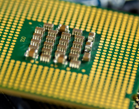
Mid-year global semiconductor sales up 20.4% compared to 2017

发布时间:2018-08-07 00:00
作者:Ameya360
来源:electroiq
阅读量:1014

The Semiconductor Industry Association (SIA), representing U.S. leadership in semiconductor manufacturing, design, and research, today announced worldwide sales of semiconductors reached $117.9 billion during the second quarter of 2018, an increase of 6.0 percent over the previous quarter and 20.5 percent more than the second quarter of 2017. Global sales for the month of June 2018 reached $39.3 billion, an uptick of 1.5 percent over last month’s total of $38.7 billion, and a surge of 20.5 percent compared to the June 2017 total of $32.6 billion. Cumulatively, year-to-date sales during the first half of 2018 were 20.4 percent higher than they were at the same point in 2017. All monthly sales numbers are compiled by the World Semiconductor Trade Statistics (WSTS) organization and represent a three-month moving average.

“Halfway through 2018, the global semiconductor industry continues to post impressive sales totals, notching its highest-ever quarterly sales in Q2 and record monthly sales in June,” said John Neuffer, president and CEO, Semiconductor Industry Association. “Global sales have increased year-to-year by more than 20 percent for 15 consecutive months, and sales of every major product category increased year-to-year in June. Sales into the Americas market continue to be strong, with year-to-date totals more than 30 percent higher than at the same point last year.”

Regionally, sales increased compared to June 2017 in China (30.7 percent), the Americas (26.7 percent), Europe (15.9 percent), Japan (14.0 percent), and Asia Pacific/All Other (8.6 percent). Sales also were up compared to last month in China (3.2 percent), Japan (1.3 percent), the Americas (1.2 percent), and Asia Pacific/All Other (0.5 percent), but down slightly in Europe (-0.8 percent).

For comprehensive monthly semiconductor sales data and detailed WSTS Forecasts, consider purchasing the WSTS Subscription Package. For detailed data on the global and U.S. semiconductor industry and market, consider purchasing the 2018 SIA Databook.

Mid-year global semiconductor sales up 20.4% compared to 2017

(备注:文章来源于网络,信息仅供参考,不代表本网站观点,如有侵权请联系删除!)

在线留言询价

相关阅读
TSMC’s U.S. Factory Plans Small-Scale Trial Line for Q1 2024
  According to a report by Taiwan’s Money DJ, the production schedule for TSMC’s semiconductor foundry in the United States has been delayed until 2025, raising concerns among observers. However, Chairman Mark Liu, in an interview on the 6th, stated that there has been significant progress over the past five months and expressed confidence in the project’s success. Industry sources have indicated that TSMC’s U.S. facility may alter its ramp-up strategy by first establishing a mini-line for trial production, with the expectation of having it in place by the first quarter of 2024.  TSMC’s Fab 21 Phase 1 construction began in April 2021, originally slated for early 2024 production. However, challenges such as a shortage of skilled equipment installation personnel, local union protests, and differences in overseas safety regulations have caused delays in equipment installation. This has compelled TSMC to adjust its plans, and the expected production timeline is now set for 2025, representing a one-year delay.  Industry analysts have noted that the efficiency of equipment entering the facility at TSMC’s U.S. plant in Arizona is only about one-third of that of its Taiwan facilities. Given the current pace of progress, the time required for equipment setup to actual production could be substantial. Therefore, TSMC has decided to change its previous ramp-up strategy and first establish a mini-line with an initial estimated monthly capacity of about 4,000 to 5,000 wafers. This approach aims to ensure some level of production output while mitigating potential contract breach issues arising from delays in production.
2023-09-08 17:00 阅读量:2976
How can semiconductor manufacturers reduce their CO2 emissions
  Semiconductor manufacturers can’t reduce CO2 emissions and energy consumption without digital technology and an end-to-end strategy  Semiconductor manufacturers are in a challenging position – they need to fulfill soaring chip demand while at the same time decarburizing their supply chain. The industry already has a giant carbon footprint and as it grows, so does its carbon footprint.  Semiconductors facilitate the ongoing shift from traditional vehicles to mobility solutions: focussing on connectivity, autonomous driving, electrification and low carbon mobility. Semiconductors help redefine mobility, reduce emissions and help alleviate congestion.  Emission reduction in vehicles and in transportation systems is made possible by semiconductor-based in-vehicle networks and sensors that increase fuel efficiency by reducing vehicle weight. Battery control and energy management semiconductor solutions extend the distance range of electric and hybrid transport and improve the predictability of that range: increased distance range is key to mass adoption of Electric vehicles.  Certain companies in the semiconductor industry have focused on sustainability for a significant period of time. ST Microelectronics and Intel have long records of focusing on water conservation and programs to reduce power. However, the Paris Accord and the recent article published in Bloomberg, accusing the semiconductor industry of having a giant carbon footprint, have initiated a new call to arms, or at least a more concerted effort on reducing the semiconductor industries carbon footprint.  Sustainability can be challenging, and while larger companies can dedicate resources to focusing on sustainability, smaller companies that support the semiconductor industry may not be able to support a dedicated Environmental Social Governance (ESG program). SEMI has picked up the ball over the past year and now is working to provide guidance and eventually standards such that the semiconductor manufacturing community can address sustainability as an industry, instead of company by company.
2023-07-17 15:04 阅读量:2970
Cutting edge transistors for semiconductors of the future
  As traditional transistors reach the threshold of their miniaturization potential, the ability to incorporate multiple functionalities within a limited number of units becomes crucial for facilitating the creation of compact, energy-efficient circuits. This, in turn, paves the way for enhanced memory capabilities and the realization of more potent computing systems.  Transistors that can change properties are important elements in the development of tomorrow's semiconductors. With standard transistors approaching the limit for how small they can be, having more functions on the same number of units becomes increasingly important in enabling the development of small, energy-efficient circuits for improved memory and more powerful computers. Researchers at Lund University in Sweden have shown how to create new configurable transistors and exert control on a new, more precise level.  Transistors that can change properties are important elements in the development of tomorrow's semiconductors. With standard transistors approaching the limit for how small they can be, having more functions on the same number of units becomes increasingly important in enabling the development of small, energy-efficient circuits for improved memory and more powerful computers. Researchers at Lund University in Sweden have shown how to create new configurable transistors and exert control on a new, more precise level.  In view of the constantly increasing need for better, more powerful and efficient circuits, there is a great interest in reconfigurable transistors. The advantage of these is that, in contrast to standard semiconductors, it is possible to change the transistor's properties after they have been manufactured.  Historically, computers' computational power and efficiency have been improved by scaling down the silicon transistor's size (also known as Moore's Law). But now a stage has been reached where the costs for continuing development along those lines has become much higher, and quantum mechanics problems have arisen that have slowed development.  Instead, the search is on for new materials, components and circuits. Lund University is among the world leaders in III-V materials, which are an alternative to silicon. These are materials with considerable potential in the development of high-frequency technology (such as parts for future 6G and 7G networks), optical applications and increasingly energy-efficient electronic components.  Ferroelectric materials are used in order to realize this potential. These are special materials that can change their inner polarization when exposed to an electric field. It can be compared to an ordinary magnet, but instead of a magnetic north and South Pole, electric poles are formed with a positive and a negative charge on each side of the material. By changing the polarization, it is possible to control the transistor. Another advantage is that the material "remembers" its polarization, even if the current is turned off.  Through a new combination of materials, the researchers have created ferroelectric "grains" that control a tunnel junction—an electrical bridging effect—in the transistor. This is on an extremely small scale—a grain is 10 nanometers in size. By measuring fluctuations in the voltage or current, it has been possible to identify when polarization changes in the individual grains and thus understand how this affects the transistor's behavior.  - The Future of the Semiconductor Industry  In addition to the upstream IC design, the midstream foundry, the DRAM industry, and the downstream packaging and testing, photomask, equipment and other industries, semiconductors have a huge group, and the application of semiconductors has also expanded to the electronic information industry, automotive electronics, Aerospace, medical, precision machinery and other industries.  While the future of the semiconductor industry looks bright, no one knows with certainty where it’s headed. The direction it moves in depends on many factors, which include the following:  · the experimentation with new semiconductor materials  · the increase in the price of rare earth metals  · the accelerated industrial adoption of new technologies in artificial intelligence (AI), the Internet of Things (IoT), and related fields  These factors and others will inevitably impact sales, create opportunities, and present fresh challenges.  At our core, we have a passion to create a better world by making electronics more affordable through semiconductors. This passion is alive today as we continue to pioneer advances in integrated circuits. Each generation of innovation builds upon the last to make technology smaller, more efficient, more reliable and more affordable. Contact us today to learn more about the services provided by Ameya360.
2023-07-11 11:46 阅读量:2796
Unlocking Compound Semiconductors’ Economy-driving Potential
  Silicon-based semiconductors and advances in computing technology have transformed our world within a short time frame. Nevertheless, we have now reached the limit of where silicon alone can take us, and innovative approaches are required for enabling the necessary advances in our digital lives.  Our collective experience with the Covid-19 pandemic has demonstrated beyond a doubt that being connected is no longer optional. Fully realizing our individual roles in this emergent, interconnected society requires us to participate via our smart devices over increasingly powerful and intertwined networks.  New technologies ranging from the internet of things, Industry 4.0, and 5G/6G to electric/autonomous vehicles and augmented reality are placing unprecedented demands on incumbent semiconductors. Rising performance requirements leave traditional silicon semiconductors unable to address the challenges.  What, then, is the solution?  A way forward is available at the level of the semiconductor materials themselves: We must look beyond silicon. And there is a group of complementary semiconductor materials that can provide the opportunity to reach where silicon cannot.  Compound semiconductors, meaning those formed from two or more elements, include materials such as gallium nitride, gallium arsenide, and indium phosphide. These semiconductors are already powering many of the technologies on which our interconnected world relies. At the same time, their adoption is rapidly accelerating (growing at double the rate of silicon), and they are becoming mainstream in power electronics, sensing, connectivity, and advanced display applications.  But the growth story does not stop there. To achieve the next wave of innovation, engineers are marrying compound semiconductors with silicon to deliver a new generation of products that will be highly disruptive in terms of the performance attributes they offer, and at a scale that will enable the mass adoption of compound semiconductors.  The growth of compound semiconductors is enabled by epitaxy, the fundamental production process used to architect atomically engineered structures from which chip companies build electronic and optoelectronic devices. By selecting the right compounds and precisely controlling how the materials are deposited on a substrate, epitaxial-wafer producers have at their disposal a unique materials “toolset” that lets them tailor wafers to enable a wide variety of device types, from power amplifiers to sensors to lasers. The level of customization that epitaxy enables is unrivaled; hence, it is the key building block of the compound-semiconductor ecosystem.  The silicon industry and its foundries have built their success upon increasingly advanced lithography techniques, mastering successive process node generations and thereby producing progressively smaller transistor technologies — 5 nm, 2 nm, and so on.  Epitaxy is to compound semiconductors what lithography is to silicon. Epitaxy thus will be central to our efforts to move beyond traditional feature scaling based on Moore’s Law.  But how does one go about turning the potential of compound semiconductors into reality — and educating an industry that is accustomed to decades of reliance on silicon-based solutions? Simply put, we need open-access foundries to start producing state-of-the-art compound semiconductors.  By way of analogy, compare Intel with TSMC in the silicon space. How many designs per month does Intel work on? One or two? Half a dozen? Now consider TSMC, which is constantly adapting its processes to various designs, forcing it to learn, adapt, and improve continuously. These “best practices” benefit everyone in the chain, from the foundry all the way to the end user.  The same situation manifests itself in the compound-semiconductor segment. Some vertically integrated chipmakers are convinced that it is optimal to produce their epitaxy in-house. However, they can never learn as fast or be as agile as an open-access foundry that is constantly collaborating with multiple customers on multiple designs. This process of building experience and knowledge gives the open-access foundry model a significant edge in the innovation race.  Further, the environmental aspects of chip manufacture can no longer be ignored. The semiconductor industry must be “carbon responsible” and minimize the lifetime impact of its materials and processes. Resources can no longer be viewed as infinite. Energy consumption has consequences. The semiconductor industry must find a way to build a digital, interconnected world that is compatible with the global push toward zero net emissions. Advanced compound-semiconductor materials are enabling the industry to innovate, and thanks to their well-documented performance and efficiency attributes versus silicon, compound semiconductors provide a key building block along the path to net zero.  I was speaking recently with several key figures from the silicon industry who echoed these trends. They increasingly recognize the importance of compound semiconductors and acknowledge the strategic importance of epitaxy. In particular, there is a recognition of the enablement that compound semiconductors provide to the silicon industry.  As a result, the silicon- and compound-semiconductor advancements are no longer separate pursuits; rather, the two industries are more significantly collaborating to deliver disruptive technologies at scale. Epitaxy plays a critical role in this work.  Semiconductors are vital to the world economy. And with an ever-increasing focus on energy efficiency and ubiquitous connectivity, compound semiconductors are poised to deliver the next-generation technology solutions that silicon simply cannot.
2023-01-10 11:02 阅读量:3023
  • 一周热料
  • 紧缺物料秒杀
型号 品牌 询价
BD71847AMWV-E2 ROHM Semiconductor
CDZVT2R20B ROHM Semiconductor
TL431ACLPR Texas Instruments
RB751G-40T2R ROHM Semiconductor
MC33074DR2G onsemi
型号 品牌 抢购
STM32F429IGT6 STMicroelectronics
ESR03EZPJ151 ROHM Semiconductor
BP3621 ROHM Semiconductor
TPS63050YFFR Texas Instruments
BU33JA2MNVX-CTL ROHM Semiconductor
IPZ40N04S5L4R8ATMA1 Infineon Technologies
热门标签
ROHM
Aavid
Averlogic
开发板
SUSUMU
NXP
PCB
传感器
半导体
相关百科
关于我们
AMEYA360微信服务号 AMEYA360微信服务号
AMEYA360商城(www.ameya360.com)上线于2011年,现 有超过3500家优质供应商,收录600万种产品型号数据,100 多万种元器件库存可供选购,产品覆盖MCU+存储器+电源芯 片+IGBT+MOS管+运放+射频蓝牙+传感器+电阻电容电感+ 连接器等多个领域,平台主营业务涵盖电子元器件现货销售、 BOM配单及提供产品配套资料等,为广大客户提供一站式购 销服务。

请输入下方图片中的验证码:

验证码