Samsung’s Big Semi Capex Spending Keeps Pressure on Competition

发布时间:2018-12-03 00:00
作者:Ameya360
来源:IC Insights
阅读量:1874

Samsung’s two-year capex spending of $46.8 billion nearly matches the combined two-year capex spending of $48.4 set by Intel and TSMC.

IC Insights revised its outlook for total semiconductor industry capital spending and presented its forecast of semiconductor capex spending for individual companies in its November Update to The McClean Report 2018, which was released earlier this month.

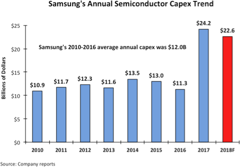
Samsung is expected to have the largest capex budget of any IC supplier again in 2018.  After spending $24.2 billion for semiconductor capex in 2017, IC Insights forecasts that Samsung’s spending will edge slightly downward, but remain at a very strong level of $22.6 billion in 2018 (Figure 1).  If it comes in at this amount, Samsung’s two-year semiconductor capital spending will be an astounding $46.8 billion.
Samsung’s Big Semi Capex Spending Keeps Pressure on Competition

Figure 1

As seen in Figure 1, Samsung’s semiconductor capital outlays from 2010, the first year the company spent more than $10 billion in semiconductor capex, through 2016 averaged $12.0 billion per year.  However, after spending $11.3 billion in 2016, the company more than doubled its 2017 capex budget.  The fact that Samsung’s continued its strong capex spending in 2018 is just as impressive.

IC Insights believes that Samsung’s massive spending outlays in 2017 and 2018 will have repercussions far into the future.  One effect that has already begun is a period of overcapacity in the 3D NAND flash market.  This overcapacity situation is due not only to Samsung’s huge spending for 3D NAND flash, but also from spending by competitors (e.g., SK Hynix, Micron, Toshiba, Intel, etc.) that attempt to keep pace in this market segment.

With the DRAM and NAND flash memory markets showing strong growth through the first three quarters of 2018, SK Hynix ramped up its capital spending this year.  In 1Q18, SK Hynix said that it intended to increase its capex spending by “at least 30%” this year.  In the November Update, IC Insights forecasts that SK Hynix will see a 58% surge in its semi capex spending.  The increased spending by SK Hynix this year is focused primarily on bringing new capacity online at two of its large memory fabs—M15, a 3D NAND flash fab in Cheongju, South Korea, and the expansion of its huge DRAM fab in Wuxi, China.  The Cheongju fab is being pushed to open before the end of this year.  The Wuxi fab is also targeted to open by the end of this year, a few months earlier than its original start date of early 2019.

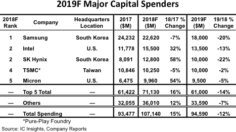
Overall, IC Insights’ now forecasts total semiconductor industry capital spending will climb 15% to $107.1 billion this year, the first time that annual industry capex is expected to top $100.0 billion.  Following the industry-wide growth this year, semiconductor capex is expected to decline 12% in 2019 (Figure 2).
Samsung’s Big Semi Capex Spending Keeps Pressure on Competition

Figure 2

Given that the current softness in the memory market is expected to extend into at least the first half of next year, the combined capital spending by the three largest memory suppliers—Samsung, SK Hynix, and Micron—is forecast to drop from $45.4 billion in 2018 to $37.5 billion in 2019, a decline of 17%.

In total, the top five spenders, which are expected to represent 66% of total outlays this year, are forecast to cut their capital spending by 14% in 2019 with the remaining semiconductor industry companies registering a 7% decline.

(备注:文章来源于网络,信息仅供参考,不代表本网站观点,如有侵权请联系删除!)

在线留言询价

相关阅读
[News] Samsung Fails to Secure Qualcomm’s 3nm Orders for the Coming Year, Dual Foundry Strategy Postponed
  According to TechNews’ report, TSMC and Samsung fiercely compete in the semiconductor foundry sector. Earlier market reports suggested that Qualcomm’s Snapdragon 8 Gen 4 mobile processor might adopt a dual-foundry strategy with TSMC and Samsung manufacturing simultaneously.  However, according to the latest industry information, due to Samsung’s conservative expansion plan for next year’s 3nm production capacity and unstable yields, Qualcomm has officially canceled the plan to utilize Samsung for next year’s processors. The dual-sourcing model is now postponed until 2025.  Samsung began mass production of its first-generation 3nm GAA (SF3E) process at the end of June last year, marking Samsung’s initial use of the innovative GAA architecture for transistor technology. The second-generation 3nm process, 3GAP (SF3), will utilize the second-generation MBCFET architecture, optimizing it based on the foundation of the first-generation 3nm SF3E. It is expected to enter mass production in 2024.  The dual-foundry strategy for Qualcomm was initially leaked by the reputable source Revegnus via the X platform (formerly Twitter). It was mentioned that the Snapdragon 8 Gen 4 processor would adopt TSMC’s 3nm (N3E) process, while Samsung’s 3GAP process would be used for the Snapdragon 8 Gen 4 supplying Samsung’s Galaxy series smartphones. Other sources suggested that due to limited capacity at TSMC’s 3nm production, Qualcomm had to seek Samsung as an alternative chip foundry.  As a result, Qualcomm originally anticipated dual-foundry production with both TSMC and Samsung in 2024, with hopes of being the first customer for the 3GAP process. However, considering Samsung’s conservative 3nm production capacity plan for next year and the instability in yields, Qualcomm decided to scrap the plan and exclusively rely on TSMC, pushing the dual-foundry strategy to 2025.  Currently, TSMC’s 3nm process technology capacity is on the rise, with expectations that by the end of 2024, monthly production capacity will reach 100,000 wafers, and the revenue contribution will increase from the current 5% to 10%.
2023-12-01 14:48 阅读量:1930
Samsung cuts NAND flash memory production
Samsung is developing next-generation memory chips for large-scale AI applications such as ChatGPT
  The large-scale application of ChatGPT and other AI chatbots will not only improve the application experience of introducing related technologies, but also bring new development opportunities to several fields, memory chip is one of them. Ameya360 reports that Samsung Electronics is exploring business opportunities by developing customized next-generation memory chips for large AI applications, such as ChatGPT, which is gaining popularity around the world.  The actual impact of ChatGPT on the chip circuit is mainly shown as follows: ChatGPT is based on Transformer technology. With the continuous iteration of the model and the increasing number of layers, the demand for computing power is increasing. Secondly, the three conditions for the operation of ChatGPT, namely, training data + model algorithm + computing power, require large-scale pre-training on the basic model. After three iterations of ChatGPT, the number of references increased from 117 million to 175 billion, and the amount of training increased significantly.  The New Computing business team of Samsung's memory business division is developing a customized next-generation memory for large-scale AI related to ChatGPT. The new computing business team, headed by Kim Jin-hyeon, is known to be a pioneer In the development of a business within the storage business division. Previously, the team focused on the development of Processing In Memory; PIM). Pims can not only store data, but also integrate and calculate data in memory, which can improve the efficiency of data processing and power consumption. Therefore, PIMs are suitable for AI.  In addition, some semiconductor industry insiders pointed out that although traditional AI chips occupy the mainstream at present and AI-dedicated chips are booming, they have met their physical limits, and the future of AI chips may be quantum chips.  Park Seong-soo, a senior researcher at the Quantum Technology Research Center at the Electronics and Communications Research Institute, said ChatGPT can also be used with a lot of computing resources, but if combined with future quantum computers, it will become a more intelligent artificial intelligence.  According to Gartner's report, total global semiconductor revenue in 2022 was approximately $601.7 billion, an increase of 1.1% year-on-year. Samsung's market share was 10.9 per cent. The ChatGPT scandal has created a new opportunity for Samsung to develop memory chips.
2023-02-21 11:26 阅读量:3606
Samsung Electronics Establishes LCA Verification on Product Carbon Footprint of Its Semiconductor Business
  Samsung Electronics Co. Ltd’s Life Cycle Assessment (LCA) on the product carbon footprint of its semiconductor business has achieved verification from DNV.  LCA is a methodology for assessing environmental impacts throughout the lifecycle of commercial products, processes, or services, by quantifying the amount of energy, materials, and waste discharge. In detail, on its semiconductors’ carbon footprint, Samsung’s LCA covers raw material extraction to chip manufacturing, assembling, and testing. Its results are in accordance with ISO 14040, ISO 14044 and ISO 14067 to ensure credibility and transparency.  The carbon footprint is commonly used by Samsung and its customers to recognize the environmental impact across all phases of Samsung’s semiconductor products, and can be used as a metric to track and reduce carbon emissions.  “Since 2019, we have been actively mobilizing efforts to measure and reduce the carbon emissions of our key memory and logic solutions,” said Dooguen Song, Executive Vice President of the Environment, Health and Safety (EHS) Center at Samsung Electronics. “By leveraging LCA, we will be able to support our customers to achieve their carbon neutrality, as well as becoming more transparent on the environmental impact of the semiconductors we produce worldwide.”  “As a global expert in energy and environmental certification, DNV is pleased to have partnered with and to congratulate Samsung on successfully establishing its reliable LCA.” said JangSup Lee, CEO of DNV Business Assurance Korea. “Together with global business leaders like Samsung, we will continue to take part in creating a more sustainable environment in the future.”  Since 2019, 37 of Samsung’s semiconductor products received carbon footprint accreditation from the Carbon Trust and UL, 6 of its memory products certified for carbon reduction from Carbon Trust. Samsung’s eco-conscious product portfolio includes DRAM, SSD, embedded storage, mobile SoC, mobile Image Sensor, automotive LED packages.  Leveraging its LCA established at the end of last year, Samsung will quantify the carbon footprints of chips manufactured across all of its global manufacturing, testing and assembly locations in Korea, China, and the U.S.  With sustainability at its core, Samsung will expand its LCA to include water and resource footprints to provide a more comprehensive assessment that will ultimately reduce the environmental impact of various applications such as mobile and wearables, data centers, consumer electronics, automotive, communications and more.
2023-02-13 15:12 阅读量:3158
  • 一周热料
  • 紧缺物料秒杀
型号 品牌 询价
BD71847AMWV-E2 ROHM Semiconductor
RB751G-40T2R ROHM Semiconductor
TL431ACLPR Texas Instruments
CDZVT2R20B ROHM Semiconductor
MC33074DR2G onsemi
型号 品牌 抢购
ESR03EZPJ151 ROHM Semiconductor
BP3621 ROHM Semiconductor
IPZ40N04S5L4R8ATMA1 Infineon Technologies
BU33JA2MNVX-CTL ROHM Semiconductor
TPS63050YFFR Texas Instruments
STM32F429IGT6 STMicroelectronics
热门标签
ROHM
Aavid
Averlogic
开发板
SUSUMU
NXP
PCB
传感器
半导体
相关百科
关于我们
AMEYA360微信服务号 AMEYA360微信服务号
AMEYA360商城(www.ameya360.com)上线于2011年,现 有超过3500家优质供应商,收录600万种产品型号数据,100 多万种元器件库存可供选购,产品覆盖MCU+存储器+电源芯 片+IGBT+MOS管+运放+射频蓝牙+传感器+电阻电容电感+ 连接器等多个领域,平台主营业务涵盖电子元器件现货销售、 BOM配单及提供产品配套资料等,为广大客户提供一站式购 销服务。