TSMC Logs First 10nm Sales

发布时间:2017-07-14 00:00
作者:Ameya360
来源:Alan Patterson
阅读量:1168

  Taiwan Semiconductor Manufacturing Co. (TSMC) has recognized its first revenue from 10nm products, trailing Samsung, its main rival in the foundry business, by nearly four months.

  TSMC said that 10 nm accounted for 1 percent of its overall revenue during the second quarter of this year. In March, Samsung announced its first 10-nm products, including the company’s Exynos 8895 SoC as well as Qualcomm's Snapdragon 835.

  TSMC expects to exit a slump that saw its second-quarter sales in dollar terms edge up just 3.2 percent from the same period a year ago. The company, which makes mobile communications products for Apple and MediaTek, said that an inventory correction among fabless customers will probably end during third quarter this year.

  “We forecast our third-quarter revenue will grow by 15.7 percent quarter on quarter,” said TSMC Co-CEO Mark Liu at an event in Taipei to announce the company’s second-quarter results. “This growth is driven by a fast ramp-up of 10-nm mobile customer products.”

  TSMC reiterated its expectation for 2017 sales growth to be in a range of 5 percent to 10 percent.

  The company may see 10 nm sales climb during the second half this year as it uses the 10 nm process to make the A11 application processor for Apple’s iPhone 8. TSMC says it expects 10 nm to account for about 10 percent of its sales during the second half of this year.

  Advanced Geometries

  The company may gain an advantage over Samsung at the 7-nm node a year from now.

  TSMC said its 7-nm yield is ahead of schedule and it expects a fast ramp in 2018. The company plans to insert several extreme ultraviolet (EUV) layers at 7 nm, but declined to provide details. The company also plans to offer a 7-nm plus node that it expects will allow customers easy migration from 7 nm.

  At this point, TSMC has about 30 tape outs for 7-nm products.

  TSMC added that its 5 nm roadmap is on track for a launch in the first quarter of 2019.

  Plugging the Gaps

  In the meantime, the company has been filling gaps in its legacy process technology to blunt the competition.

  TSMC has increased capacity for its 28 nm process, which accounted for more than a quarter of its revenue during the second quarter this year. The company, which has counted on 28 nm as a cash cow for more than five years, is hanging on to a 90 percent share of the market even as rivals such as Intel are trying to grab a chunk of that business.

  “We aim to achieve full capacity at all nodes,” said Co-CEO CC Wei. “We believe we are the lowest-cost supplier.”

  TSMC has introduced a 22-nm node between the 28 and 16-nm geometries that the company currently offers.

  TSMC aims to offer 12 nm products based on its 16 nm technology after it completes 12 nm development work in the second half of this year. The 12 nm technology will be an “optical shrink” of 16 nm, which will allow customers to convert existing 16 nm designs easily, according to Wei.

  Even so, there are some niches where TSMC plays second fiddle. At the 20/16 nm node, TSMC has faced strong competition from Samsung, which makes 14 nm products for Qualcomm.

  Sales of TSMC’s 16/20 nm products dropped to 26 percent in the second quarter, sliding from 31 percent of total first quarter revenue and 33 percent during the fourth quarter of 2016. TSMC expects the 16/20 nm decline to continue during the third quarter this year.

(备注:文章来源于网络,信息仅供参考,不代表本网站观点,如有侵权请联系删除!)

在线留言询价

相关阅读
Intense Competition in Advancing Processes at the 2nm by Samsung, Intel, and TSMC
  According to TechNews’ report, Gitae Jeong, Vice President of Samsung Electronics, recently revealed in an interview that the company is set to introduce the SF1.4 (1.4nm) process, expected to enter mass production in 2027.  This announcement intensifies the competition in advanced semiconductor manufacturing, particularly in the development of 2.5D/3D integrated heterogeneous structure packaging among the three major semiconductor foundry giants.  *TSMC: N3P Process Superior to Intel 18A, N2 to Lead Industry’s Advanced Processes  Previously, the semiconductor industry reported challenges with both TSMC and Samsung achieving yields above 60% for their 3nm processes due to undisclosed issues. TSMC’s yield was reported to be only 55%, below the normal yield rate.  However, TSMC’s President, C.C. Wei, expressed optimism, stating that current N3 demand is better than three months ago, contributing to a healthy growth outlook for TSMC in 2024.  Wei also anticipates that TSMC’s 3nm process will contribute a mid-single-digit percentage (4%-6%) to the company’s annual wafer revenue in 2023.  Regarding competition with rival Intel’s 18A process, Wei believes that TSMC’s N3P process offers better performance, power, and area (PPA), alongside improved cost efficiency and technical maturity. Furthermore, TSMC’s upcoming N2 process is expected to be the industry’s most advanced when introduced.  *Intel: Striving for the Fourth Customer for 18A Process Outsourcing Orders  Intel’s CEO, Pat Gelsinger, has revealed that the 18A process has secured orders from three customers and aims to acquire a fourth customer by the end of the year. The advanced 18A process is scheduled to begin production at the end of 2024, with one customer already having made an advance payment. External expectations suggest that the customer could possibly be NVIDIA or Qualcomm.  Intel has stated that Intel 4 and Intel 3 processes are similar, as are Intel 20A and Intel 18A processes. Consequently, Intel’s primary focus will be on offering Intel 3 and Intel 18A to semiconductor foundry customers. Meanwhile, Intel 4 and Intel 20A processes are more likely to be used internally. However, Intel is open to accommodating customer requests if they express interest in adopting these later processes.  *Samsung: Commencing Mass Production of SF2 in 2025, Prioritizing Internal Use  Due to challenges with the three-nanometer (3nm) manufacturing process, there have been reports that Samsung plans to shift directly to the more advanced two-nanometer (2nm) process.  According to Samsung’s Foundry Forum (SFF) plan, they will begin mass production of the 2nm process (SF2) in 2025 for mobile applications, expand to high-performance computing (HPC) applications in 2026, and further extend to the automotive sector and the expected 1.4nm process by 2027.  Similar to Intel, Samsung intends to prioritize the production of its own products using the 2nm process. The 2nm process products will initially be utilized for Samsung’s in-house products rather than external customer products.  *Summary  While TSMC’s N3 series currently enjoys broad support, including N3E, N3X, and N3P process series, the move to 2nm introduces new variables as it adopts a completely new GAAFET architecture. Regardless, whether it’s TSMC’s N2, Intel’s 18A, or Samsung’s SF2, each of them possesses its competitive strengths. The industry is also eagerly anticipating the future developments in advanced semiconductor processes.
2023-11-03 14:50 阅读量:1449
TSMC’s Capacity and Orders Surge, Is the Semiconductor Industry Bouncing Back?
  As reported by China Taiwanese media, there’s a gradual uptick in TSMC’s capacity utilization lately, accompanied by a noticeable surge in orders from TSMC’s clients. Some segments of the market are showing signs of rekindled demand, hinting at a possible upswing in the semiconductor industry. Nevertheless, certain semiconductor manufacturing firms remain cautious in their industry outlook.  TSMC’s Capacity Utilization Rate on the Rise  Media’s report indicates that TSMC’s capacity utilization rate has gradually recovered. The 7/6nm utilization, which had dropped to 40% at one point, is now around 60% and could potentially reach 70% by the end of the year. Similarly, the 5/4nm utilization is at 75-80%, and the 3nm capacity, which increases seasonally, is approximately 80%.  Concurrently, TSMC is experiencing a significant uptick in orders from their clients, including tech giants like Apple, MediaTek, NVIDIA, AMD, Intel, Broadcom, Marvell, and STMicroelectronics. Furthermore, AI chip clients such as AMD’s subsidiary Xilinx, Amazon, Cisco, Google, Microsoft, and Tesla have all accepted TSMC’s plan for a price increase in 2024.  Taking Tesla as an example, they are building a supercomputer facility in Austin to accelerate the development of their autonomous driving system, expanding the computing power of Dojo. The core D1 of Dojo is produced using TSMC’s 7nm process and advanced packaging technology. Based on this, Tesla is deepening its collaboration with TSMC, and it’s expected that their order volume will increase from around 5,000 pieces this year to 10,000 pieces next year.  Amid the ongoing AI surge, NVIDIA is actively seeking additional production capacity. On October 19th, NVIDIA’s CEO, Jensen Huang, revealed in an interview that the global demand for AI chips remains robust. He has met with TSMC’s CEO, C.C. Wei, to discuss providing more capacity to serve customers. NVIDIA is in the planning stages for the next generation of chips designed for AI-based infrastructure and has also engaged in discussions with partners such as Quanta and ASUS to strategize collaboration.  Is the Semiconductor Industry on the Rebound?  During TSMC’s Q3 earnings call, C.C. Wei pointed out that, in addition to strong AI demand, there’s a rebound in demand for smartphones and personal computers. As for automotive electronics, benefiting from the continued growth of electric vehicles, the demand for next year is expected to be quite robust. Regarding when the semiconductor industry might hit bottom, Wei remarked that there are some early signs appearing in the PC and mobile phone sectors. However, it remains challenging to predict a strong resurgence as customers are still cautiously managing their inventories.  In response to industry concerns about smartphone growth, TSMC’s CFO, Wendell Huang, noted that smartphone growth is anticipated to remain lower than the company’s future growth rate. High-Performance Computing (HPC) is expected to be the most robust growth segment, making substantial contributions to growth in the coming years.  On the other hand, other semiconductor foundry companies, such as PSMC, have also shared their perspectives on the fourth quarter and future industry developments. Recently, PSMC’s President, Brian Shieh, pointed out that the supply chain’s inventory seems to have reached a reasonable level, with growing demand for mobile panel driver ICs, surveillance system CIS chips, and visibility extending beyond one quarter. Prices for special memory products have started to show an upward trend. Demand for Power Management ICs (PMIC) also displays signs of recovery, even though the trend isn’t as pronounced as that of driver ICs and CIS chips.  Regarding UMC, the company is scheduled to hold an earning call on 25th October. In their previous earnings call for the last quarter, UMC mentioned that due to ongoing adjustments in the supply chain’s inventory, the outlook for wafer demand remains uncertain. Although the industry glimpsed a modest recovery in the second quarter, the overall sentiment in the end-market remains subdued, and customers continue to maintain stringent inventory management practices.
2023-10-25 11:18 阅读量:1416
Intel, Samsung, TSMC Race in Cutting-Edge Processes
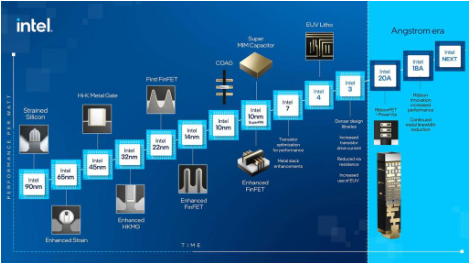
  Driven by emerging technologies like AI and high-performance computing, the semiconductor foundry industry increasingly emphasizes the importance of advanced manufacturing processes. Recently, the industry has seen significant developments. Intel announced that it has commenced large-scale production of its Intel 4 process node, while TSMC and Samsung are equally committed to advancing their advanced process technologies.  Intel’s Mass Production of Intel 4 Process Node  On October 15th, Intel China’s official public account revealed that Intel has initiated large-scale production of the Intel 4 process node using Extreme Ultraviolet Lithography (EUV) technology. According to Intel, they are making significant progress with their “Four Years, Five Nodes” plan. This plan aims to produce next-generation products that meet the computational demands driven by AI’s role in the “Siliconomy.”  Being the first process node produced by Intel using EUV lithography technology, Intel 4 offers substantial improvements in performance, efficiency, and transistor density compared to its predecessors. Intel 4 was unveiled at the Intel Innovation 2023 held in September this year.  In comparison to Intel 7, Intel 4 achieves a 2x reduction in area, providing high-performance computing (HPC) logic libraries and incorporating various innovative features.  In detail, Intel 4 simplifies the EUV lithography process, optimizing it for high-performance computing applications, supporting both low voltage (<0.65V) and high voltage (>1.1V) operations. Compared to Intel 7, Intel 4 boasts more than a 20% improvement in iso-power performance, and high-density Metal-Insulator-Metal (MIM) capacitors deliver outstanding power supply performance.  Intel’s “Four Years, Five Nodes” plan is advancing with the following process updates:  Intel 7 and Intel 4 are currently in large-scale production. Intel 3 is on track to meet its planned target by the end of 2023.  Intel’s Intel 20A and Intel 18A, which use Ribbon FET all-around gate transistors and PowerVia backside power delivery technology, are also progressing well, with a target of 2024. Intel will soon introduce the Intel 18A process design kit (PDK) for Intel Foundry Services (IFS) customers.  With the adoption of Intel 4 process nodes, the Intel Core i9 Ultra processor, codenamed “Meteor Lake,” will be released on December 14th this year, ushering in the AIPC era.  On Intel 3 process nodes, the energy-efficient E-core Sierra Forest processor will be launched in the first half of 2024, and the high-performance P-core Granite Rapids processor will follow closely.  Samsung’s 2nm Process Detailed Production Plan  Samsung has already commenced production of its second-generation 3nm chips and plans to continue focusing on 2nm chips.  On June 28th, Samsung Electronics unveiled its latest foundry technology innovations and business strategies at the 7th Samsung Foundry Forum (SFF) in 2023.  In the era of artificial intelligence, Samsung’s foundry program, based on advanced GAA process technology, offers robust support for customers in AI applications. To this end, Samsung has disclosed a detailed production plan and performance levels for its 2nm process. The plan is to achieve mass production for mobile applications by 2025 and respectively expand to HPC and automotive electronics in 2026 and 2027.  Samsung reports that the 2nm process (SF2) improves performance by 12% compared to the 3nm process (SF3), increases efficiency by 25%, and reduces the area by 5%.  Furthermore, reports indicated that Samsung is ensuring the production capacity for products using the next-generation EUV lithography machine, High-NA, in September. This equipment is expected to have a prototype by the end of this year and officially enter production next year.  TSMC’s Mass Production of 2nm by 2025  This year, TSMC has unveiled its latest advanced semiconductor manufacturing roadmap in various locations, including Santa Clara, California, and Taiwan. The roadmap covers a range of processes from 3nm to 2nm.  TSMC’s current roadmap for 3nm includes N3, N3E, N3P, N3X, and N3 AE, with N3 serving as the foundational version, N3E as an enhanced version with further cost optimization, N3P focusing on improved performance with a planned start in the second half of 2024, N3X targeting high-performance computing devices with a mass production goal in 2025, and N3 AE designed specifically for the automotive sector, offering greater reliability and the potential to shorten time-to-market by 2-3 years.  In the 2nm realm, TSMC is planning to achieve mass production of the N2 process by 2025. TSMC has reported that the N2 process will offer a 15% speed improvement over N3E at the same power or a 30% reduction in power consumption, with a 15% increase in transistor density. In September, media reports revealed that TSMC has formed a task force to accelerate 2nm pilot production and mass production, aiming for risk production next year and official mass production in 2025.  To ensure the smooth development of 2nm process technology, TSMC has initiated efforts in the upstream equipment sector. On September 12th, TSMC announced the acquisition of a 10% stake in IMS Nanofabrication, a subsidiary of Intel, for a price not exceeding $432.8 million. IMS specializes in the research and production of electron beam lithography machines, which find extensive applications in semiconductor manufacturing, optical component manufacturing, MEMS manufacturing, and more. The industry sees TSMC’s IMS acquisition as vital for developing crucial equipment and meeting the demand for 2nm process commercialization.
2023-10-18 13:12 阅读量:1407
TSMC Expected to Lower Capital Expenditure, Potentially Falling Below $30 Billion for the Year
  As TSMC’s earnings call approaches, the market is abuzz with rumors that the company may revise down its capital expenditure target for this year. This potential adjustment is believed to be driven by delays in Intel’s 3-nanometer outsourcing and the deferral of the production schedule for TSMC’s 4-nanometer US fab. The initial capital expenditure target, which was close to the $32 billion to $36 billion range, may now be lowered to below $30 billion, marking its lowest point in nearly three years.  According to Taiwan’s Economic Daily, TSMC has refrained from commenting on these speculations. Even if TSMC does adjust its capital expenditure for this year, industry sources suggest that the company will increase its annual R&D expenses, continuing its commitment to advanced research and development.  In recent years, TSMC has rapidly expanded its capital expenditure, reaching a record high of $36.3 billion last year. In the first half of this year, the actual capital expenditure amounted to $18.11 billion, including $8.17 billion in the second quarter, slightly down from the $9.94 billion in the first quarter.  During their July earnings conference, TSMC stated that their capital expenditure for the year would remain in the range of $32 billion to $36 billion. However, considering market dynamics, the actual expenditure for the full year is expected to be towards the lower end of this range.  The latest reports suggest that due to the delays in Intel’s 3-nanometer outsourcing and the postponement of the 4-nanometer production schedule at the US fab, approximately $4 billion originally earmarked for this year’s capital expenditure may be postponed until next year, resulting in capital expenditure for this year falling below $30 billion. As for next year’s capital expenditure, it may remain on par with this year.  ASML, a leading supplier of semiconductor lithography equipment, previously revealed in its July earnings conference that there were delays in shipments of EUV equipment due to installation delays at customer factories. However, ASML maintained a robust order backlog and expects overall performance to continue growing in 2024.  Industry experts believe that the “installation delays” mentioned by ASML at that time were related to TSMC, and because of the delay in EUV equipment installation, TSMC’s capital expenditure for this year may be deferred accordingly.  Analysts in the industry suggest that if we consider TSMC’s earlier projection of capital expenditure falling within the $32 billion to $36 billion range, and subtract the actual expenses incurred in the first half of the year, the capital expenditure for the second half of the year could see a decline, estimated to be around $13.89 billion or more. If the postponement rumors materialize, second-half capital expenditure might fall below $10 billion.
2023-10-17 11:03 阅读量:1549
  • 一周热料
  • 紧缺物料秒杀
型号 品牌 询价
CDZVT2R20B ROHM Semiconductor
RB751G-40T2R ROHM Semiconductor
BD71847AMWV-E2 ROHM Semiconductor
TL431ACLPR Texas Instruments
MC33074DR2G onsemi
型号 品牌 抢购
BP3621 ROHM Semiconductor
STM32F429IGT6 STMicroelectronics
TPS63050YFFR Texas Instruments
ESR03EZPJ151 ROHM Semiconductor
IPZ40N04S5L4R8ATMA1 Infineon Technologies
BU33JA2MNVX-CTL ROHM Semiconductor
热门标签
ROHM
Aavid
Averlogic
开发板
SUSUMU
NXP
PCB
传感器
半导体
相关百科
关于我们
AMEYA360微信服务号 AMEYA360微信服务号
AMEYA360商城(www.ameya360.com)上线于2011年,现 有超过3500家优质供应商,收录600万种产品型号数据,100 多万种元器件库存可供选购,产品覆盖MCU+存储器+电源芯 片+IGBT+MOS管+运放+射频蓝牙+传感器+电阻电容电感+ 连接器等多个领域,平台主营业务涵盖电子元器件现货销售、 BOM配单及提供产品配套资料等,为广大客户提供一站式购 销服务。

请输入下方图片中的验证码:

验证码