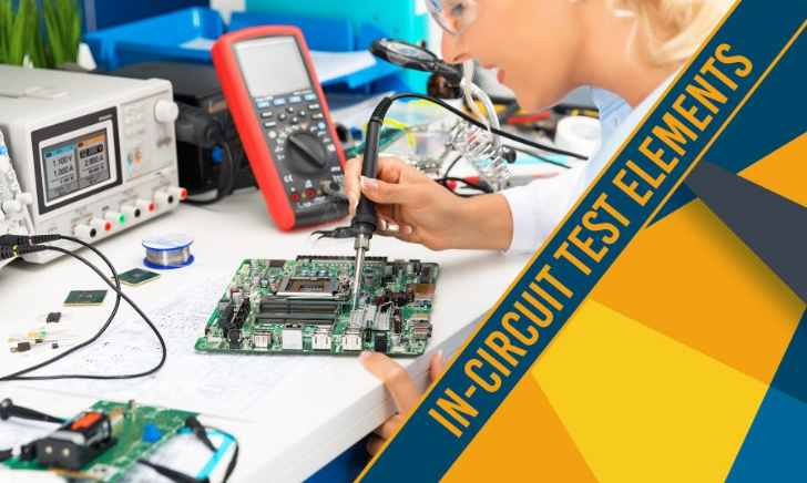
Ameya360:How In-circuit Test Elements Make PCB Testing Easier

发布时间:2023-01-20 13:34
作者:Ameya360
来源:网络
阅读量:1882

  The growing complexity of electronic designs is challenging the PCB manufacturing industry to innovate PCB inspection and testing methodologies. To bring out reliable products with maximum yield, a variety of inspection and test methods are employed during the PCB manufacturing process. In-circuit testing (ICT) is used to detect flaws in manufacturing processes and components. It offers high fault coverage and quick test throughput as compared to other available test methodologies. The ICT diagnostic accuracy is exceptional with low incorrect fail rates.

Ameya360:How In-circuit Test Elements Make PCB Testing Easier

  The introduction of the ICT system shifted the focus from the functionality testing of the PCB to the testing of components’ functionality and the integrity of the assembly process. This largely simplified the test pattern generation as the understanding of complex board functionality was eliminated for the programmer. A bed-of-nails test fixture used in the ICT method allows electrical test access to every net on the PCB and enables stimulating and measuring each component independently. This method has significantly reduced the time to generate test vectors and has improved the quality of the test coverage.

  Elements of In-Circuit Test:

  There are multiple types of ICT machines available in the market. Based on the test process, types of PCBs, and production volume you can choose the machine for your requirement. The basic elements of an ICT machine are as follows:

  In-circuit tester: A bed-of-nails used as drivers and sensors that are inserted on pins of the device under test (DUT). They are used to apply voltage and current to the device pins to measure electrical parameters like impedance, capacitance, and resistance of the circuit.

  Fixture: A fixture is designed specifically for a PCB and acts as an interface between the board and the In-circuit tester. It connects the test stimulus and monitoring points to the corresponding pins on the board through bed-of-nails.

  Software: It is the set of test vectors generated specific to a board based on the type of tests to be done. It also provides control of the test process by collecting data from the probes. A pass or fail criteria is generated and applied while testing the PCBs. Test reports are generated that can assist in troubleshooting the faults.

  Apart from the standard ICT machines, there are some advanced variants like Flying probe testers that can accommodate board updates by changing software, Cable form testers optimized to test cables, and Manufacturing defect analyzers that can spot defects like short and open circuits on the printed circuit board assembly.

  Faults detected using ICT machines

  The test coverage offered by the in-circuit tester is diverse. Manufacturers perform both power-off and power-on tests using ICT machines.

  PCB defects detected in power-off mode are:

   Shorts between component pins and traces

   Resistor values

   Missing passive or analog parts

   Correct jumper settings

   Opens with no electrical connectivity

   Lifted leads

   Solder bridge

   BGA shorts and opens

  Also, PCB defects captured during power-on mode are:

   Capacitance and inductance values

   Misorientation of mounted analog and digital parts

   Current gain value (beta) of the transistors

   Timing parameters of digital components

   Programming error of memory devices

       Merits of in-circuit testing

  ICT has made PCB testing easier by offering several advantages as below:

  Easy program generation without the need to understand the board functionality has significantly reduced the test development time.

  Since the setup can access all nets and component pins of the circuit board, the test coverage is maximum as compared to other PCB test methods.

  Minimal scope for operator error as the manual intervention required is limited.

  Quick fault detection and simple interpretation of error saves test and debug time for the operator.

  Detects both assembly and functional faults of the PCB.

  Software can operate on both UNIX and windows OS

  Many tests performed in power-off mode provide a safer testing method for PCBs and hence reduced damage.

  Once installed, ICT setups require minimal maintenance as they are robust and operate reliably for years.

  Development in ICT systems

  There are several improvements in the latest ICT systems. The possible erosion of test point access on PCBs, diverse test case requirements for products, and demand for high yield in volume productions are addressed. With the development in test strategies, the In-circuit test method is also progressing to provide excellent test coverage for PCB assemblies.

  ICT vendors are offering scalable ICT test systems to satisfy diverse test requirements in a single compatible platform. For addressing high-volume manufacturing requirements, some ICT systems support parallel testing of components on the board. High-accuracy probe-fixturing technologies are available today that can establish smaller yet reliable test points.

  The cost of the test fixture is quite high and the profit depends on the build volume. It is more suitable for medium to high-volume PCB production. High board complexity and dimensions will add to the cost as the fixture density and size also increase. But the reliability and test coverage offered by this technique compensates for the other drawbacks.

  Compared to the flying probe test method, the In-circuit test is faster. Its ability to test for both assembly and functional defects makes it a better choice in large-volume testing. ICT can perform sophisticated tests specified in the Joint Test Action Group (JTAG) standards. Since the fixtures are built specifically for the test boards, it has to be done only after the PCB layout is finalized. The complexity involved in building the test fixtures calls for a substantial amount of time and money from the overall production budget.

  Conclusion

  To identify the best test strategy for your PCB assembly, it is necessary that you collaborate with an experienced contract manufacturer. They can offer guidance based on your specific needs with a complete understanding of the test strategies. For prototypes or low-volume PCB assembly, ICT is not recommended. The PCB must be in the production phase with a complete design freeze. It is ideal to build test fixtures for production PCBs since there are no re-spins expected.  Also, to recover the cost of test infrastructure, it is ideal to use ICT in bulk PCB productions.


(备注:文章来源于网络,信息仅供参考,不代表本网站观点,如有侵权请联系删除!)

在线留言询价

相关阅读
Difference between Diode and Triode in PCBA manufacturing
  In printed circuit board assembly (PCBA) manufacturing, understanding the differences between diode and triode is crucial for designing efficient electronic circuits. Both components play essential roles in controlling the flow of electrical current, but they have distinct characteristics that determine their specific applications and functionalities.  Diode:Diode  A diode is a two-terminal electronic component that primarily allows current to flow in one direction while blocking it in the opposite direction. Here are key characteristics and uses of diodes in PCBA manufacturing:  1. Functionality: Diodes are used for rectification, converting AC (Alternating Current) to DC (Direct Current). They ensure that current flows in only one direction, preventing reverse polarity which can damage sensitive components.  2. Types: Common types include:  – Rectifier Diodes: Used in power supplies to convert AC to DC.  – Zener Diodes: Maintain a constant voltage for regulation.  – Light-Emitting Diodes (LEDs): Emit light when current flows through them, used for indicators and displays.  3. Applications: Diodes are found in almost all electronic circuits:  – Power supplies  – Signal demodulation  – Overvoltage protection  – Voltage regulation  Triode (Transistor):Triode  A triode, also known as a transistor, is a three-terminal semiconductor device that amplifies or switches electronic signals and electrical power. Here are the key characteristics and uses of triodes in PCBA manufacturing:  1. Functionality: Triodes can amplify current, acting as switches or amplifiers depending on the configuration:  – Bipolar Junction Transistors (BJTs): Amplify current and are used for analog circuits.  – Field-Effect Transistors (FETs): Control current flow with an electric field, used in digital circuits.  2. Types: Different types cater to specific applications:  – NPN and PNP BJTs: Common bipolar transistor types.  – MOSFETs (Metal-Oxide-Semiconductor Field-Effect Transistors): High-speed switching in digital circuits.  – JFETs (Junction Field-Effect Transistors): Used in amplifiers and analog switches.  3. Applications: Triodes are essential in modern electronics:  – Amplifiers in audio systems  – Switching circuits in digital logic gates  – Oscillators in radio frequency applications  – Drivers for motors and relays  Comparison– Function: Diodes primarily control current direction, whereas triodes amplify or switch currents.  – Configuration: Diodes are two-terminal devices, while triodes (transistors) have three terminals: emitter, base, and collector.  – Applications: Diodes are crucial for power supply and signal processing, while triodes are fundamental in amplification and digital switching.  In conclusion, while diodes and triodes are both essential components in PCBA manufacturing, their distinct functionalities and applications make them suitable for different roles within electronic circuits. Understanding their differences is key to designing and assembling efficient and reliable electronic devices.
2024-08-16 14:24 阅读量:362
What is “component placement” in PCB?
  Component placement is a critical step in the PCB assembly process where electronic components are precisely positioned and soldered onto the printed circuit board (PCB). This phase plays a crucial role in ensuring the functionality, reliability, and performance of the final electronic device. Let’s delve into the details of component placement in PCB assembly.  How many electronic components are there?1. Surface Mount Devices (SMDs):  – Passive Components: Resistors, capacitors, inductors.  – Active Components: Integrated circuits (ICs), transistors, diodes.  2. Through-Hole Components:  – Components with leads that pass through holes drilled in the PCB.  What is the component placement process?1. Design for Assembly (DFA)  Before physical assembly begins, the PCB layout and design must consider DFA principles:  – Component Orientation: Optimizing orientation for ease of assembly and efficient routing of traces.  – Clearance and Spacing: Ensuring adequate space for soldering and avoiding interference between components.  – Accessibility: Facilitating automated or manual assembly processes.  2. Automated Component Placement  Modern PCB assembly typically involves automated pick-and-place machines:  – Vision Systems: Cameras identify fiducial markers or component outlines on the PCB to align and place components accurately.  – Component Feeding: Components are loaded into feeders, which supply them to the pick-and-place machine.  – Pick-and-Place Process: The machine picks components from the feeder using vacuum nozzles, aligns them precisely over corresponding pads on the PCB, and places them gently using controlled motion.  3. Manual Component Placement  For specialized components or low-volume production, manual placement may be used:  – Skill and Precision: Technicians use hand tools like tweezers and magnifiers to place components accurately.  – Prototype Builds: Initial prototypes or small batches may benefit from manual placement for flexibility and customization.  What should be considered when placing components in PCB?Component placement is more than just arranging components on a board; it involves strategic decisions that impact the overall functionality and quality of the PCB. Proper placement not only ensures that the circuit operates correctly but also affects signal integrity, thermal management, and ease of assembly. Here are some crucial aspects to consider:  1. Design for Signal Integrity  Signal integrity is crucial for the proper operation of high-speed digital circuits and sensitive analog circuits. To maintain signal integrity:  – Minimize Trace Length: Place critical components closer together to minimize trace lengths, reducing signal delay and electromagnetic interference (EMI).  – Signal Paths: Follow a logical signal flow from input to output, avoiding crossing high-speed signals with noisy or high-current traces.  – Grounding: Ensure a solid ground plane and place components that require low impedance connections to ground strategically to minimize noise and ground loops.  2. Thermal Management  Certain components, such as power transistors or voltage regulators, generate heat during operation. Efficient thermal management is essential to prevent overheating and ensure reliability:  – Heat Sinks: Provide adequate space and mounting locations for heat sinks or thermal pads.  – Airflow: Arrange components to allow natural or forced airflow across heat-generating components.  – Isolation: Keep heat-sensitive components away from those generating significant heat to prevent thermal damage.  3. Manufacturability and Assembly  Designing for manufacturability involves ensuring that the PCB can be efficiently assembled with minimal errors and rework:  – Component Accessibility: Ensure components are placed such that they can be easily soldered by hand or by automated pick-and-place machines.  – Orientation: Align components consistently for ease of assembly and to avoid errors during soldering.  – Clearance and Spacing: Adhere to manufacturing guidelines for minimum clearance between components, ensuring soldering and inspection can be done without issues.  4. Electromagnetic Compatibility (EMC)  PCB layout plays a crucial role in achieving EMC compliance by reducing EMI emissions and susceptibility:  – Component Arrangement: Position sensitive components and traces to minimize loop areas and coupling.  – Shielding: Group and shield sensitive components from noise sources such as high-current paths or switching circuits.  – Grounding and Routing: Properly route and ground signal return paths to reduce loop areas and impedance discontinuities.  Best Practices for Component Placement– Start with Critical Components: Begin by placing critical components such as microcontrollers, connectors, and high-frequency components based on their functional and spatial requirements.  – Use Design Tools: Leverage PCB design software with simulation capabilities to visualize signal paths, analyze thermal performance, and optimize placement before fabrication.  – Iterative Refinement: Iterate the placement based on simulation results, design reviews, and practical considerations to achieve the best balance of performance and manufacturability.  – Documentation: Clearly label components with reference designators and polarity markings on the silkscreen layer. Maintain an updated BOM (Bill of Materials) to ensure accurate procurement and assembly.  ConclusionComponent placement in PCB assembly is a pivotal stage where careful planning, advanced technology, and skilled craftsmanship converge to create reliable electronic devices. By adhering to DFA principles, leveraging automation, and considering thermal and signal integrity factors, manufacturers can achieve efficient, high-quality assembly that meets the demands of today’s electronics industry. As technology advances, component placement continues to evolve, driving innovation and pushing the boundaries of what’s possible in electronic design and manufacturing.
2024-07-18 11:48 阅读量:524
15 Common PCB Circuit Effects
  Printed Circuit Boards (PCBs) are the backbone of modern electronics, serving as the foundation for countless devices we rely on daily. However, designing and working with PCBs come with its own set of challenges and nuances. In this guide, we delve into 15 common circuit effects that engineers and enthusiasts encounter when designing and troubleshooting PCBs.  Each effect explored here sheds light on a specific aspect of PCB design, whether it’s related to signal integrity, power distribution, or electromagnetic interference. Through concise explanations and practical examples, we aim to equip readers with a deeper understanding of these effects, enabling them to optimize their PCB designs for performance, reliability, and manufacturability.  Whether you’re a seasoned electronics engineer or a hobbyist diving into the world of PCB design, this guide is designed to serve as a valuable reference, helping you navigate the intricacies of PCB circuits with confidence and expertise.  1. Drawbridging effectIn high-density wiring, when there is not enough space between two lines, a situation may occur where one line hangs over another line, similar to the shape of a suspension bridge.  The drawbridging effect usually occurs in PCB design, especially in cases where a large number of signal lines need to be arranged and space is limited. The drawbridging effect may lead to problems such as signal crosstalk, electromagnetic interference, signal distortion, or delay.  Measures to reduce the drawbridging effect:  Reasonably plan the PCB layout, try to keep the signal lines arranged in a straight line, and avoid situations where lines cross or overlap.  Optimize PCB routing, try to increase the spacing between signal lines as much as possible to avoid the suspension bridge effect caused by too small spaces.  Use layered PCB design to arrange different signal lines on different layers to reduce crossing and interference between lines.  Reduce electromagnetic interference between signal lines by appropriate signal layer and ground layer planning to improve the circuit’s anti-interference ability.  2. Ripple effectIn high-speed circuits, when the signal transmission speed is fast, the signal may undergo ripple deformation when propagating on the PCB, affecting the signal quality, including signal distortion, clock offset, crosstalk, and interference.  Measures to reduce ripple effects:  Optimize PCB layout and routing to minimize the bending, crossing, and branching of signal lines, and maintain the consistency of signal transmission paths.  Adopt appropriate signal line and ground design to reduce crosstalk and interference between signal lines, improving signal transmission quality.  Use signal compensation or pre-emphasis technology to compensate for and enhance the signal, reducing waveform distortion and deformation.  Choose appropriate signal transmission lines and signal processing devices to improve the circuit’s anti-interference ability and transmission speed.  3. Overshoot effectSudden voltage changes that occur during signal transmission may cause excessive voltage shock to components on the circuit board, damaging components or causing circuit failures.  Overshoot effects may be caused by excessively fast rising or falling edges of the signal, or by the instability of the signal transmission line or signal source.  Measures to reduce overshoot effects:  Optimize the design of signal transmission lines to ensure the impedance matching and stability of the signal lines.  Use appropriate power filters and power decoupling capacitors to reduce interference from signal sources.  Adopt signal pre-emphasis technology or signal compensation technology to preprocess or compensate the signal, reducing the occurrence of overshoot effects.  Choose appropriate components and circuit protection devices to improve the circuit’s resistance to overshoot and stability.  4. Resonance effectParameters such as inductance, capacitance, and impedance on the circuit board may cause resonance of the signal at specific frequencies, affecting the stable transmission of the signal. This resonance phenomenon usually occurs at specific frequencies when the frequency of external signals matches the resonant frequency of the circuit, causing resonance effects.  Measures to reduce resonance effects:  Optimize PCB layout and design to avoid situations where the circuit has a resonant frequency close to the excitation frequency.  Use compensation circuits or filters to eliminate or suppress resonance effects.  Choose appropriate damping components or damping materials to reduce the impact of resonance effects.  Adopt appropriate circuit tuning techniques to stabilize the circuit’s frequency response within a specific frequency range.  5. Floating EffectIn high-speed circuits, due to factors such as electromagnetic radiation, signals may float on the surface of conductors or circuit boards, affecting signal transmission and reception.  To reduce the impact of PCB floating effect on circuits, designers can take the following measures:  Measures to Reduce Floating Effect:  Optimize PCB layout and design, plan the routing and spacing of signal lines reasonably, and minimize the impact of electromagnetic radiation on signal transmission.  Use appropriate signal line and ground line designs to ensure impedance matching and stability of signal lines.  Use shielding covers or shielding materials to reduce electromagnetic radiation and interference.  Select suitable PCB materials and components to reduce the occurrence of floating effects.  6. Crosstalk EffectDue to factors such as dense layout of PCB signal lines or electromagnetic interference, different signal lines may experience crosstalk. Crosstalk can lead to degradation of signal quality or abnormal circuit function.  Measures to Reduce Crosstalk Effect:  Optimize PCB layout and design, plan the routing and spacing of signal lines reasonably, and minimize mutual interference between signal lines.  Use shielding covers, shielding materials, or ground isolation techniques to reduce the impact of electromagnetic interference on signals.  Use differential signal transmission lines or increase signal layers to improve anti-interference capability and reduce the occurrence of crosstalk.  Select suitable PCB materials and components to reduce the impact of crosstalk effects.  7. Reflection EffectRefers to the phenomenon in high-speed signal transmission where signals encounter impedance mismatch or incomplete absorption of signal energy by the terminal of the signal transmission line, resulting in signals reflecting back to the original source end. This reflection effect may cause signal waveform distortion, affecting the transmission quality and stability of the circuit.  Measures to Reduce Reflection Effect:  Design signal transmission lines reasonably to ensure impedance matching and minimize impedance mismatch situations.  Use terminal resistors or terminal capacitors to absorb signal energy and reduce signal reflection.  Optimize PCB layout and design to minimize the length of signal transmission lines and reduce signal transmission delay.  Select suitable PCB materials and components to reduce the impact of reflection effects.  8. Shielding EffectThe metal layer or shielding cover on the PCB may shield signals, affecting the transmission range and quality of signals.  Measures to Reduce Shielding Effect:  Design PCB layout reasonably: Try to avoid overlap or proximity between signal lines and shielding areas to minimize the impact of shielding effect.  Choose appropriate shielding materials: Select suitable metal layers or shielding cover materials in PCB design to have good shielding performance while minimizing the impact on signal transmission.  Design suitable grounding structure: A good grounding structure can help reduce the shielding effect of signals and improve signal transmission quality.  Pay attention to signal adjustment: For signals that need to pass through shielding areas, signal adjustment techniques can be employed to minimize the impact of shielding effect, such as increasing signal power or adjusting signal transmission methods.  9. Thermal Expansion EffectTemperature changes may cause thermal expansion or contraction of PCB materials, affecting the dimensional stability of circuit boards and the connection status of components.  Measures to Reduce Thermal Expansion Effect:  Choose appropriate PCB materials: Selecting PCB materials with smaller coefficients of thermal expansion can reduce the impact of thermal expansion on circuits.  Design PCB layout reasonably: During PCB design, try to avoid direct connection between materials with high coefficients of thermal expansion and those with low coefficients to reduce the impact of thermal expansion.  Control soldering temperature: Control soldering temperature and time during the soldering process to avoid excessive temperature leading to solder joint failure or component displacement.  Use support structures: Adding appropriate support structures in PCB design can reduce PCB bending deformation, improving the stability and reliability of the PCB.  10. Ground Hole EffectThere are many ground holes on the PCB. When ground holes are close to signal lines or other ground holes, ground hole effect may occur, affecting the stability of signal transmission.  Measures to Reduce Ground Hole Effect:  Design ground holes reasonably: Design appropriate parameters for ground holes, such as diameter, pitch, copper foil diameter, etc., to ensure impedance matching and consistency of ground holes, reducing ground hole inductance and crosstalk effects.  Use ground hole filling: Ground hole filling techniques can be employed in PCB design to fill ground holes, reducing their impact on signal transmission and improving PCB performance stability.  Optimize layout: Plan PCB layout reasonably to minimize the number and density of ground holes, reducing their impact on circuits.  Adjust interlayer stacking: Choose PCB layer stacking methods appropriately to minimize ground holes between inner and outer layers, reducing the impact of ground hole effect.  11. Filling EffectThe filling material on the PCB may affect signal transmission. For example, differences in the dielectric constant of the filling material may cause changes in signal transmission speed or signal attenuation.  Measures to Reduce Filling Effect:  Choose filling material reasonably: Select filling materials with a dielectric constant close to that of the PCB material to reduce the impact of dielectric constant differences on signal transmission.  Control the thickness of filling material: Properly control the thickness of filling material to avoid excessive thickness, which could lengthen the signal transmission path and increase attenuation.  Optimize PCB layout: During PCB design, minimize the impact on signal transmission paths, plan filling areas reasonably, and avoid interference from filling materials on signal transmission paths.  Use low-loss filling materials: Choose filling materials with low resistance and dielectric loss to minimize attenuation and distortion during signal transmission.  12. Temperature Drift EffectTemperature changes on the PCB may cause thermal expansion or contraction of circuit board materials, thereby affecting the dimensional stability of the circuit board and the connection status of components.  Measures to Reduce Temperature Drift Effect:  Choose PCB materials reasonably: Select PCB materials with good thermal stability and dimensional stability to reduce the impact of temperature changes on the PCB.  Control soldering temperature: During the soldering process, control soldering temperature and time properly to avoid excessive soldering temperature leading to damage or breakage of components and solder joints.  Optimize PCB layout: Plan PCB layout reasonably to reduce differences in thermal expansion coefficients between components and avoid changes in the connection status of components due to temperature changes.  Temperature environment control: Control temperature changes in the PCB usage environment to avoid significant temperature shocks to the PCB, thereby reducing the impact of temperature changes on PCB circuits.  13. Crystal EffectDevices such as transistors in PCB routing may be influenced by the surrounding environment, causing changes in device parameters and affecting circuit performance.  Measures to Reduce Crystal Effect:  Rational Layout: Properly plan PCB layout to avoid external interference affecting devices such as transistors and minimize electromagnetic field interference with devices.  Temperature Control: Take measures to control the operating temperature of the PCB board during design and manufacturing to reduce the influence of temperature changes on device parameters and improve circuit stability.  Choose Appropriate Devices: Select transistors and other devices with good anti-interference and stability to reduce the impact of crystal effect on the circuit.  Design Compensation Circuits: In PCB design, compensation circuits can be used to correct drift in device parameters, improving circuit performance and stability.  14. Restricted EffectThere are some restricted areas on the PCB, such as edges, power supply areas, etc., which may impose certain limitations or impacts on signal transmission or routing.  Measures to Reduce Restricted Effect:  Rational Planning of Layout: During PCB design, plan the layout reasonably to avoid placing sensitive signal lines or components near restricted areas, reducing the impact of restrictions.  Electromagnetic Shielding: For areas prone to electromagnetic interference in restricted areas, electromagnetic shielding measures can be adopted, such as placing metal shielding covers around sensitive areas to reduce the impact of external electromagnetic interference on the circuit.  Optimization of Power Supply Design: For possible power supply instability or noise issues in power supply areas, measures such as optimizing power supply design, adding filtering circuits, and reducing power supply noise can be taken to improve power supply stability and circuit performance.  Fine Routing: When routing in restricted areas, adopt fine routing methods as much as possible to reduce restrictions or elongation of signal transmission paths, improving signal transmission rate and stability.  15. Landmine EffectHidden problems or faults on PCB boards may suddenly appear during subsequent testing or use, causing unexpected impacts or damage to the circuit board.  Measures to Reduce Landmine Effect:  Strict Quality Control: During PCB production, strictly control the quality of each process to ensure that each component and circuit connection meets specifications, reducing hidden dangers.  Perfect Testing Procedures: Establish comprehensive testing and inspection procedures to conduct comprehensive testing and inspection of PCB circuits, promptly identify and repair potential problems.  Use Reliable Components: Choose components and materials with high reliability and stable quality to reduce the probability of failure and minimize the occurrence of landmine effects.  Strengthen Maintenance: Regularly maintain and upkeep produced PCB circuits, promptly identify and repair potential problems, improving circuit reliability and stability.
2024-04-30 10:11 阅读量:455
What is the difference between the package substrate and PCB
  The packaging substrate is a kind of electronic substrates that can provide electrical connection, protection, support, heat dissipation, assembly and other functions for chips and electronic components, so as to achieve multi-pin, reduce the volume of packaged products, improve electrical performance and heat dissipation, ultra-high density or multi-chip modularization and high reliability.  The packaging substrate can be considered as a PCB or thin-thick film circuit substrate with higher performance or special functions. The packaging substrate plays the role of electrical interconnection and transition between the chip and the conventional printed circuit board (mostly motherboard, sub-board, backplane, etc.), and also provides protection, support, heat dissipation, assembly and other functions for the chip.  With the continuous progress and development of electronic installation technology, the boundaries of various levels of electronic installation are becoming less and less clear. The role of PCB is becoming more and more important. Higher and newer requirements are put forward for PCB and its substrate materials in terms of function and performance.  Difference between package substrate and PCB  Printed Circuit Board (PCB) refers to a circuit board that forms a copper circuit pattern on a copper clad laminate according to a predetermined design. Its main function is to connect various electronic components according to a predetermined circuit and act as an electrical connection.  The packaging substrate and PCB manufacturing principles are similar. It is the extension of PCB to high-end technology to adapt to the rapid development of electronic packaging technology. There is a certain correlation between the two. The packaging substrate is a high-end PCB.  package substrate  In electronic packaging engineering, the electronic substrate (PCB) can be used for different levels of electronic packaging (mainly used for the 2nd to 5th levels of the 1st to 3rd level packaging), but the packaging substrate is used for the 2nd and 3rd levels of the 1st and 2nd level packaging, Ordinary PCBs are used for levels 3, 4, and 5 of level 2 and level 3 packages.  However, they all provide functions such as interconnection, protection, support, heat dissipation, and assembly for electronic components to achieve multi-pin, reduce the volume of packaged products, improve electrical performance and heat dissipation, ultra-high density or multi-chip modularization, and high reliability for the purpose.  The process and reasons for the separation of the package substrate from the PCB  After the 1980s, with the wide application of new materials and new equipment, integrated circuit design and manufacturing technology developed rapidly in accordance with “Moore’s Law”, tiny and sensitive semiconductor components came out, large-scale integrated circuits and ultra-large-scale integrated circuits appeared, and high-density multilayer packaging substrates emerged as the times require, which separates integrated circuit packaging substrates from ordinary printed circuit boards. A proprietary manufacturing technology for integrated circuit packaging substrates then formed.  At present, among the mainstream products of conventional PCB boards, products with a line width/line spacing of 50μm/50μm belong to high-end PCB products. However, this technology still cannot meet the technical requirements of the current mainstream chip packaging. In the field of packaging substrate manufacturing, products with a line width/line spacing of 25μm/25μm have become more common, which reflects that packaging substrate manufacturing is more advanced in technology than conventional PCB manufacturing.  There are two fundamental reasons for the separation of packaging substrates from conventional printed circuit boards: on the one hand, because the development speed of PCB boards is lower than that of chips, it is difficult to directly connect chips and PCB boards. On the other hand, the cost of the PCB board refinement is much higher than the cost of interconnecting the PCB and the chip through the packaging substrate.  Main structure and production technology of package substrate  At present, there is no unified classification standard in the packaging substrate industry. Packaging substrate is usually classified according to the substrate material and manufacturing technology applicable to substrate manufacturing.  According to different substrate materials, packaging substrates can be divided into inorganic packaging substrates and organic packaging substrates. Inorganic packaging substrates mainly include: ceramic-based packaging substrates and glass-based packaging substrates. Organic packaging substrates mainly include: phenolic packaging substrates, polyester packaging substrates, and epoxy resin packaging substrates.  Organic Package Substrate  According to the different manufacturing methods of the packaging substrate, the packaging substrate can be divided into a core packaging substrate and a new coreless packaging substrate.  Core and coreless packaging substrates  The core package substrate is mainly divided into two parts in structure, the middle part is the core board, and the upper and lower parts are laminated boards. The production technology of the core packaging substrate is based on the high-density interconnection (HDI) printed circuit board production technology and its improved technology.  Core and coreless packaging substrates  A coreless substrate refers to a packaging substrate with a core board removed. The fabrication of the new coreless package substrate mainly produces interlayer conductive structures—copper pillars—by bottom-up electrodeposition technology. It only uses an insulating layer (Build-up Layer) and a copper layer to achieve high-density wiring through a semi-additive (SemiAdditive Process, abbreviated as SAP) build-up process.  Advantages and disadvantages of coreless packaging substrates  Advantages  Thinning;  The electrical transmission path is reduced, the AC impedance is further reduced, and its signal line effectively avoids the return loss generated by the PTH (copper plated through hole) on the traditional core substrate, which reduces the inductance of the power system loop and improves the transmission. characteristics, especially frequency characteristics;  The direct transmission of signals can be realized, because all circuit layers can be used as signal layers, which can improve the freedom of wiring, realize high-density wiring, and reduce the limitation of C4 layout;  Except for some processes, the original production equipment can be used, and the process steps are reduced.  Disadvantages  Without core board as support, it is easy to warp and deform in the manufacture of coreless substrates, which is the most common and biggest problem at present;  Laminate shattering is prone to occur;  Some new equipment for coreless substrates for semiconductor packaging needs to be introduced. Therefore, the challenges of coreless substrates for semiconductor packaging mainly lie in materials and processes.
2024-03-14 17:12 阅读量:748
  • 一周热料
  • 紧缺物料秒杀
型号 品牌 询价
RB751G-40T2R ROHM Semiconductor
MC33074DR2G onsemi
TL431ACLPR Texas Instruments
CDZVT2R20B ROHM Semiconductor
BD71847AMWV-E2 ROHM Semiconductor
型号 品牌 抢购
STM32F429IGT6 STMicroelectronics
ESR03EZPJ151 ROHM Semiconductor
IPZ40N04S5L4R8ATMA1 Infineon Technologies
BP3621 ROHM Semiconductor
TPS63050YFFR Texas Instruments
BU33JA2MNVX-CTL ROHM Semiconductor
热门标签
ROHM
Aavid
Averlogic
开发板
SUSUMU
NXP
PCB
传感器
半导体
相关百科
关于我们
AMEYA360微信服务号 AMEYA360微信服务号
AMEYA360商城(www.ameya360.com)上线于2011年,现 有超过3500家优质供应商,收录600万种产品型号数据,100 多万种元器件库存可供选购,产品覆盖MCU+存储器+电源芯 片+IGBT+MOS管+运放+射频蓝牙+传感器+电阻电容电感+ 连接器等多个领域,平台主营业务涵盖电子元器件现货销售、 BOM配单及提供产品配套资料等,为广大客户提供一站式购 销服务。

请输入下方图片中的验证码:

验证码