- Ameya360 Component Supply Platform >
- Trade news >
- What is LED packaging? Principles of LED packaging
What is LED packaging? Principles of LED packaging
LED packaging is an essential element in the world of lighting technology. It involves the process of encapsulating and protecting delicate LED components, allowing them to deliver high-performance illumination in a range of applications. With its compact size, energy efficiency, and long lifespan, LED packaging has revolutionized the way we illuminate our surroundings. In this article, we will talk about what is LED packaging, its importance, its principles, and general packaging methods.
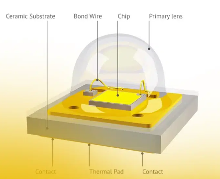
What is LED packaging?
LED packaging refers to assembling LED chips and other components (such as connecting wires and packaging materials) together to form a complete LED lamp. The purpose of LED packaging is to enable the LED chip to work properly in practical applications and have sufficient brightness and stability.
Why is LED packaging needed?Generally speaking, the function of packaging is to protect the chip, extend the stability of the chip’s normal operation, and prevent the chip from being corroded by impurities in the air or mechanical damage from the outside and unable to continue to be used when exposed to the air for a long time. Specifically, the functions of LED packaging mainly include: 1. Mechanical protection to improve reliability; 2. Enhance heat dissipation to reduce chip junction temperature and improve LED performance; 3. Optical control to improve light extraction efficiency and optimize beam distribution; 4. Power supply management, including AC/DC conversion, power control, etc.
Principles of LED packagingThe principle of LED packaging can be divided into the following steps:
1. Preparation of LED chips: LED chips are the core components of LED lights and need to be prepared through chemical reactions and physical techniques. LED chips are usually made of two materials: n-type semiconductor and p-type semiconductor. The two materials form a PN junction through a chemical reaction. When a voltage is applied through the LED’s connecting wire, electrons and holes combine in the PN junction and generate photons, thereby emitting light.
2. Install electrodes and connecting wires: LED chips need to be installed with electrodes and connecting wires in order to transmit electrical signals to the chip. The electrodes and connecting wires are usually made of metal and can be fixed to the chip by soldering or bonding.
3. Packaging materials: Packaging materials are the key to combining LED chips and other components. Packaging materials usually have good waterproof properties, insulation properties and high temperature resistance. The packaging material can be materials such as plastic, glass or ceramic. The selection of packaging materials needs to be determined based on the purpose and application environment of the LED lamp.
4. Packaging process: The packaging process is to assemble the LED chip and other components together to form a complete LED lamp. The packaging process usually includes the following steps: placing the LED chip in the packaging material, fixing the electrodes and connecting wires, pouring the packaging material, heating and curing the packaging material. During the packaging process, attention needs to be paid to the uniformity and thickness of the packaging material to ensure the brightness and stability of the LED light.
To sum up, LED packaging is the process of combining LED chips and other components to form a complete LED lamp. The principle of LED packaging includes steps such as preparing LED chips, installing electrodes and connecting wires, packaging materials and packaging processes. Through scientific and reasonable packaging design and manufacturing technology, high-quality, high-brightness, and high-stability LED lights can be obtained.
What are the general packaging methods?The selection of LED packaging methods, materials, structures and processes is mainly determined by factors such as chip structure, optoelectronic/mechanical characteristics, specific applications and costs. After more than 40 years of development, LED packaging has successively gone through development stages such as Lamp LED, SMD LED, and Power LED. With the increase in chip power, especially the demand for the development of solid-state lighting technology, new and higher requirements have been put forward for the optical, thermal, electrical and mechanical structures of LED packages. In order to effectively reduce the thermal resistance of the package and improve the light extraction efficiency, new technical ideas must be adopted for package design.
After more than 40 years of development, LED packaging technology and structure have gone through four stages.
1. Pin-type (Lamp) LED packaging
The pin-type package is the commonly used A3-5mm package structure. Generally used for LED packages with smaller current (20-30mA) and lower power (less than 0.1W). It is mainly used for instrument display or indication, and can also be used as a display screen during large-scale integration. The disadvantage is that the package thermal resistance is large (generally higher than 100K/W) and the life is short.
2. Surface assembly (SMT-LED) packaging
Surface mounting technology (SMT) is a packaging technology that can directly attach and solder packaged devices to designated positions on the PCB surface. Specifically, specific tools or equipment are used to align the chip pins on the pad pattern that has been pre-coated with adhesive and solder paste, and then directly mounted on the PCB surface without drilling mounting holes, and then undergo wave soldering. Or after reflow soldering, a reliable mechanical and electrical connection is established between the device and the circuit. SMT technology has the advantages of high reliability, good high-frequency characteristics, and easy automation. It is the most popular packaging technology and process in the electronics industry.
3. Chip-on-board (COB) LED packaging
COB is the abbreviation of Chip On Board. It is a packaging technology that directly pastes the LED chip onto the PCB board through adhesive or solder, and then realizes the electrical interconnection between the chip and the PCB board through wire bonding. The PCB board can be made of low-cost FR-4 material (glass fiber reinforced epoxy resin), or it can be a metal-based or ceramic-based composite material with high thermal conductivity (such as an aluminum substrate or copper-clad ceramic substrate, etc.). Wire bonding can use thermosonic bonding at high temperatures (gold wire ball bonding) and ultrasonic bonding at room temperature (aluminum cleaver welding). COB technology is mainly used for LED packaging of high-power multi-chip arrays. Compared with SMT, it not only greatly improves the packaging power density, but also reduces the packaging thermal resistance (generally 6-12W/mK).
4. System in package (SiP) LED packaging
SiP (System in Package) is a new packaging integration method developed on the basis of System on Chip (SOC) in recent years to adapt to the portable development and miniaturization requirements of the entire machine. For SiP-LED, not only can multiple light-emitting wafers be assembled in one package, but also various types of devices (such as power supplies, control circuits, optical microstructures, sensors, etc.) can be integrated together to build a more complex and complete system. Compared with other packaging structures, SiP has good process compatibility (existing electronic packaging materials and processes can be used), high integration, low cost, can provide more new functions, is easy to be tested in blocks, and has a short development cycle. Etc. According to different technology types, SiP can be divided into four types: chip stack type, module type, MCM type and three-dimensional (3D) packaging type.
Online messageinquiry
- Week of hot material
- Material in short supply seckilling
| model | brand | Quote |
|---|---|---|
| RB751G-40T2R | ROHM Semiconductor | |
| TL431ACLPR | Texas Instruments | |
| CDZVT2R20B | ROHM Semiconductor | |
| BD71847AMWV-E2 | ROHM Semiconductor | |
| MC33074DR2G | onsemi |
| model | brand | To snap up |
|---|---|---|
| IPZ40N04S5L4R8ATMA1 | Infineon Technologies | |
| BP3621 | ROHM Semiconductor | |
| STM32F429IGT6 | STMicroelectronics | |
| BU33JA2MNVX-CTL | ROHM Semiconductor | |
| ESR03EZPJ151 | ROHM Semiconductor | |
| TPS63050YFFR | Texas Instruments |
- Week of ranking
- Month ranking
Qr code of ameya360 official account
Identify TWO-DIMENSIONAL code, you can pay attention to


Please enter the verification code in the image below:


