- Ameya360 Component Supply Platform >
- Trade news >
- What is a multilayer thick film ceramic PCB
What is a multilayer thick film ceramic PCB
In the ever-evolving world of electronics, Printed Circuit Boards (PCBs) form the basis of modern devices. Among the latest innovations, multilayer thick film ceramic PCBs have emerged as a breakthrough technology, revolutionizing electronic design and performance. In this comprehensive article, we will explore the world of multilayer thick film ceramic PCBs and learn about their unique features, benefits, and how they differ from other types of ceramic PCBs.
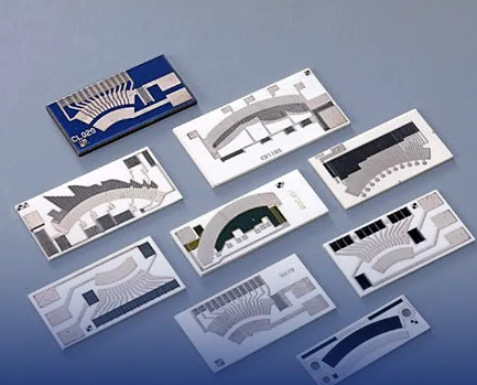
What is a multilayer thick film ceramic PCB?Multilayer thick film ceramic PCB is an advanced type of printed circuit board that uses specialized ceramic materials with embedded thick film conductive traces. This is a method of forming conductive traces and electrodes by screen printing on a substrate, directly depositing a slurry and sintering it at high temperatures. This method is suitable for most ceramic substrates. After sintering at high temperature, it will form a strong adhesion film on the ceramic circuit board, and after many repetitions, a multi-layer interconnection structure containing resistor or capacitor circuits will be generated.
Multilayer thick film ceramic PCBs are also known as hybrid thick film ceramic circuits, but one important difference between them is that hybrid thick film technology has resistors on its surface, while multilayer thick film ceramic only has conductors.
Other types of ceramic PCBsWith the rapid development of the electronic field, there are a total of 6 types of ceramic PCBs on the market, and different technologies have their own unique characteristics. Let’s have a brief look at them.
DPC ceramic PCB
DPC ceramic PCB, also known as direct copper-clad ceramic PCB, is a printed circuit board made of ceramic materials, in which the copper layer is directly plated on the ceramic substrate. Based on thin film technology, the metallization of the ceramic surface can be achieved through magnetron sputtering. The thickness of the electric copper layer is greater than 10 microns, and the thickness can be increased through electroplating. This technology offers several advantages over traditional copper-clad PCBs.
DBC ceramic PCB
Featuring a copper layer bonded directly to the ceramic substrate, DBC ceramic PCBs are known for their excellent thermal conductivity and are suitable for high-power applications such as inverters and motor drives. Since DBC ceramic PCBs are made by sintering, the conductor thickness can exceed 100 microns (up to 300 microns). Unlike DPC ceramic PCB, DBC technology cannot be designed with through holes or vias as this would affect the insulation function.
AMB ceramic PCB
The full name of AMB is active metal brazing technology, which is a further development of DBC technology. Its working principle is to use active metal elements (such as Ti/Ag/Zr/Cu) in brazing to achieve the combination of ceramics and metals. In terms of performance, bonding in AMB ceramic substrates is achieved through the chemical reaction of ceramic and reactive metal solder at temperature. The Si3N4 ceramic used in AMB has higher thermal conductivity (>90W/mK 25℃) than traditional Al2O3 ceramic substrate, which is close to the thermal expansion coefficient of silicon (2.6×10 -6 /K), so the AMB substrate has higher adhesion Strength and reliability.
HTCC Ceramic PCB
HTCC ceramic circuit boards are manufactured at high temperatures (approximately 1300°C) so they can withstand extreme temperatures and have excellent thermal stability. They are commonly used in aerospace, telecommunications and high-reliability applications. Its use is limited due to its complex manufacturing process and expensive raw materials.
LTCC ceramic PCB
Unlike HTCC ceramic boards, LTCC PCBs are processed at lower temperatures (about 850℃~1000℃), allowing the integration of passive components and are widely used in radio frequency and microwave modules, sensors and telecommunications fields. Like multilayer thick film ceramic PCBs, both HTCC and LTCC technologies can manufacture multilayer PCBs.
How are multilayer thick film ceramics different from other types?Multilayer thick film ceramics are very different from other types of ceramic PCBs. The biggest difference is that thick film technology can print resistors on its surface. As the technology matures, we can make all resistors the same value, or design different values for different resistors on the same board. At the same time, using thick film technology, we can place resistors, capacitors, conductors, semiconductors and interchangeable conductors on ceramic boards, after the manufacturing steps of printing and high-temperature sintering.
However, limited by the size of the conductive paste and screen, the minimum trace width of thick film ceramics is difficult to be less than 60 microns (0.6 mm), and it is impossible to create three-dimensional graphics, so it is not suitable for the production of fine circuit boards.
The conductors of thick film ceramic circuits can be gold paste and silver paste (other pastes need to be evaluated). Under normal circumstances, the sintering temperature is 850°C, but if glass glaze is required as a soldering cap layer, the sintering temperature should be about 600°C.
Online messageinquiry
What is “component placement” in PCB?
15 Common PCB Circuit Effects
- Week of hot material
- Material in short supply seckilling
| model | brand | Quote |
|---|---|---|
| BD71847AMWV-E2 | ROHM Semiconductor | |
| RB751G-40T2R | ROHM Semiconductor | |
| MC33074DR2G | onsemi | |
| TL431ACLPR | Texas Instruments | |
| CDZVT2R20B | ROHM Semiconductor |
| model | brand | To snap up |
|---|---|---|
| IPZ40N04S5L4R8ATMA1 | Infineon Technologies | |
| BP3621 | ROHM Semiconductor | |
| ESR03EZPJ151 | ROHM Semiconductor | |
| TPS63050YFFR | Texas Instruments | |
| STM32F429IGT6 | STMicroelectronics | |
| BU33JA2MNVX-CTL | ROHM Semiconductor |
- Week of ranking
- Month ranking
Qr code of ameya360 official account
Identify TWO-DIMENSIONAL code, you can pay attention to


Please enter the verification code in the image below:

