common electronic components and their symbols

发布时间:2023-11-07 15:22
作者:AMEYA360
来源:network
阅读量:1283

  When it comes to electronics, there are numerous components that are essential to building any functional circuit. Here are 10 common electronic components that you’re likely to encounter.
common electronic components and their symbols

  Resistor

  Resistor will cause a change in the flow of electrons. The smaller the resistance, the greater the flow of electrons, and vice versa. Substances with no resistance or very little resistance are called electrical conductors, or conductors for short. Substances that cannot form electric current transmission are called electrical insulators, or insulators for short.

  In physics, resistance is used to represent the size of the conductor’s resistance to current flow. The greater the resistance of the conductor, the greater the resistance of the conductor to current flow. Different conductors generally have different resistances, and resistance is a characteristic of the conductor itself. Resistive elements are energy-dissipating elements that impede current flow.

  Resistor symbol: Resistor is represented by “R” plus numbers in the circuit, such as: R1 represents the resistance numbered 1. The main functions of resistors in the circuit are shunting, current limiting, voltage dividing, biasing, etc.

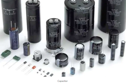
  Capacitor

  Capacitance refers to the charge storage capacity under a given potential difference; denoted as C, and the international unit is farad (F). Generally speaking, charges will move under force in an electric field. When there is a medium between conductors, it will hinder the movement of charges and make charges accumulate on the conductors; the accumulation and storage of charges is caused. The most common example is two parallel metal plates. It is also commonly known as a capacitor.

  Inductor

  Inductance is a property of a closed circuit and a physical quantity. When the coil passes current, a magnetic field induction is formed in the coil, and the induced magnetic field will generate an induced current to resist the current passing through the coil. Inductors are inductive components made of inductive properties.

  If the inductor is in a state where no current is flowing, it will try to block the current from flowing through it when the circuit is on; if the inductor is in a state where current is passing, it will try to maintain the current when the circuit is off. Inductors are also called chokes, reactors, and dynamic reactors.

  Inductor symbol: Inductor is often represented by “L” plus numbers in the circuit, such as: L6 represents the Inductor numbered 6.

  Crystal Diode

  A crystal diode is a semiconductor two-terminal device in solid-state electronic devices. The main feature of these devices is their nonlinear current-voltage characteristics.

  Since then, with the development of semiconductor materials and process technology, a variety of crystal diodes with various structures and functions have been developed using different semiconductor materials, doping distributions, and geometric structures. Manufacturing materials include germanium, silicon and compound semiconductors. Crystal diodes can be used to generate, control, receive, transform, amplify signals, and perform energy conversion.

  Crystal diode symbol: Crystal diodes are often represented by “D” plus numbers in circuits, such as: D5 represents a diode numbered 5.

  Zener Diode

  Zener diode is a semiconductor device with high resistance until the critical reverse breakdown voltage.

  The Zener diode is a diode that uses the reverse breakdown state of the pn junction, and its current can change in a wide range while the voltage is basically unchanged. It is a diode that acts as a voltage regulator. The diode is a semiconductor device with high resistance up to a critical reverse breakdown voltage.

  At this critical breakdown point, the reverse resistance decreases to a very small value, and the current increases while the voltage remains constant in this low-resistance region. Zener diodes are graded according to their breakdown voltage. Because of this characteristic, Zener diodes are mainly used as voltage regulators or voltage reference components. Zener diodes can be connected in series for use at higher voltages, and higher stable voltages can be obtained through series connection.

  Zener diode symbol: Zener diodes are often represented by “ZD” plus numbers in the circuit, such as: ZD5 means a Zener diode numbered 5.

  Varactor Diode

  Varactor diodes, also known as ‘variable reactance diodes’, are made by utilizing the characteristics that the junction capacitance changes with the applied voltage when the pN junction is reverse-biased. It is used as a variable capacitor in high-frequency tuning, communication and other circuits. It is used in high-frequency circuits for automatic tuning, frequency modulation, tuning, etc., for example, as a variable capacitor in the tuning circuit of a TV receiver.

(备注:文章来源于网络,信息仅供参考,不代表本网站观点,如有侵权请联系删除!)

在线留言询价

相关阅读
What are the different types of electronics components packages?
  In the realm of electronics, various packaging technologies cater to the diverse needs of components, ensuring functionality, compactness, and performance. These packaging methods are crucial in determining a component’s size, compatibility, and usage in different applications. Here, we delve into some of the most prevalent component packaging technologies shaping the electronic landscape:  1. Through-Hole Technology (THT)Through-Hole Technology (THT): DIP (Dual In-line Package), SIP (Single In-line Package), TO (Transistor Outline), etc.  Through-Hole Technology (THT) is a method used to mount and connect electronic components to a printed circuit board (PCB). In THT, leads (metal wires) extend from the electronic component and are inserted into pre-drilled holes on the PCB. Once inserted, the leads are soldered to pads on the opposite side of the board, forming a secure electrical and mechanical connection.  Components suitable for THT include resistors, capacitors, diodes, and integrated circuit sockets, among others. THT was one of the primary assembly methods for electronic components before the rise of Surface Mount Technology (SMT), which introduced smaller and more densely packed components suitable for automated assembly.  2. Surface Mount Technology (SMT)Surface Mount Technology (SMT): SOIC (Small Outline Integrated Circuit), QFP (Quad Flat Package), LGA (Land Grid Array), BGA (Ball Grid Array), etc.  Surface Mount Technology (SMT) is a method used in electronic assembly to mount and solder components directly onto the surface of a printed circuit board (PCB). In contrast to Through-Hole Technology (THT), which involves inserting component leads through holes in the PCB, SMT components have small metallic contacts or leads that sit directly on the board’s surface. SMT components are generally smaller and more compact than their through-hole counterparts, allowing for higher component densities and smaller PCB designs.  SMT components include resistors, capacitors, integrated circuits (ICs), diodes, and other semiconductor devices. The process involves soldering the components to the PCB’s surface using reflow soldering, where solder paste is applied to the board, and then the components are placed on the paste. The entire assembly is heated, causing the solder to melt and create a secure connection between the component leads and the PCB pads.  Surface Mount Technology has become the dominant method in modern electronics manufacturing due to its efficiency, miniaturization capabilities, and suitability for automated assembly processes.  3. Ball Grid Array (BGA)  Ball Grid Array (BGA): μBGA (Micro Ball Grid Array), CCGA (Ceramic Column Grid Array), PBGA (Plastic Ball Grid Array), etc.  Ball Grid Array (BGA) is a type of surface mount packaging used for integrated circuits (ICs) and other semiconductor devices. It’s characterized by an array of solder balls arranged in a grid formation on the underside of the component. These solder balls serve as the connection points to the PCB.  However, working with BGAs requires specialized equipment and techniques for both assembly and rework due to the complexity of soldering the numerous small solder balls. Nonetheless, they are widely used in various applications, especially in high-performance computing, gaming consoles, networking hardware, and consumer electronics, where space and performance are critical considerations.  4. Chip Scale Packaging (CSP)  Chip Scale Packaging (CSP): mCSP (micro Chip Scale Package), WLP (Wafer-Level Package), FC-CSP (Flip Chip Chip Scale Package), etc.  Chip Scale Packaging (CSP) refers to a packaging technology for integrated circuits (ICs) where the package size closely matches the dimensions of the silicon die or chip itself. In essence, CSPs aim to minimize the footprint of the package while providing the necessary protection and connections for the chip.  CSPs are commonly used in portable electronic devices such as smartphones, tablets, wearables, and other miniaturized gadgets. Their small form factor and efficient use of space make them ideal for applications demanding high-performance chips in constrained areas.  5. Quad Flat Packages (QFP)  Quad Flat Packages (QFP): TQFP (Thin Quad Flat Package), PQFP (Plastic Quad Flat Package), LQFP (Low-profile Quad Flat Package), etc.  Quad Flat Packages (QFP) are a type of surface mount integrated circuit package characterized by a flat body and leads extending from all four sides of the component. The leads are arranged in a grid pattern, allowing for easy soldering to the printed circuit board (PCB).  QFPs were a popular choice for integrating moderate-to-high pin counts in a compact form factor before more miniaturized packages, such as Ball Grid Arrays (BGAs) and Chip Scale Packages (CSPs), gained prominence in the electronics industry.  6. Plastic Leaded Chip Carrier (PLCC)  Plastic Leaded Chip Carrier (PLCC): PQFP (Plastic Quad Flat Package), LQFP (Low-profile Quad Flat Package), etc.  A Plastic Leaded Chip Carrier (PLCC) is a type of integrated circuit (IC) package used for surface-mounted devices. It’s a square or rectangular package made of plastic with metal leads extending from the sides. PLCC packages typically contain a semiconductor chip and have leads or pins on all four sides, which are used for connection to a circuit board.  PLCCs have largely been replaced by smaller and more efficient packages like quad flat no-leads (QFN) and ball grid arrays (BGAs) in many modern electronic devices due to their higher pin density, smaller footprint, and improved electrical performance.  7. Transistor Outline (TO) Packages  Transistor Outline (TO) Packages: TO-92, TO-220, TO-263, TO-220AB, etc.  Transistor Outline (TO) packages are a standardized type of packaging used for discrete semiconductor components like transistors and some integrated circuits. These packages are designed to provide a standardized form factor for easy handling, mounting, and heat dissipation.  The TO packages are convenient for manual or automated assembly onto circuit boards, and their standardized dimensions make them easily interchangeable in various electronic designs. However, due to advancements in technology, smaller and more efficient packages like surface-mount devices (SMDs) are becoming more prevalent in modern electronic designs, reducing the use of TO packages in some applications.  8. Dual Flat No-Lead (DFN) Packages  Dual Flat No-Lead (DFN) Packages: WDFN (Thin Dual Flat No-Lead), SON (Small Outline No-Lead), QFN (Quad Flat No-Lead), etc.  Dual Flat No-Lead (DFN) packages are a type of surface-mount semiconductor package used for integrated circuits (ICs), such as microcontrollers, integrated power devices, and sensors. The DFN package is characterized by its small size, low profile, and absence of leads or pins extending from the package sides.  DFN packages have a flat bottom with exposed metal pads arranged in a grid pattern. The electrical connections are made by soldering these pads directly onto corresponding pads on the surface of a printed circuit board (PCB). The absence of leads makes DFN packages suitable for high-density mounting, as they occupy less space and offer improved electrical performance due to shorter interconnection paths.  DFN packages are popular in modern electronic devices where miniaturization and efficient use of space are crucial design considerations. Their compact size, good thermal performance, and ability to accommodate higher pin counts make them favored choices in many consumer electronics, telecommunications, and portable devices.  9. Small Outline Package (SOP)  Small Outline Package (SOP): TSOP (Thin Small Outline Package), SSOP (Shrink Small Outline Package), HSOP (Heatsink Small Outline Package), etc.  The Small Outline Package (SOP) is a type of surface-mount technology used for integrated circuits. SOP packages are characterized by their rectangular shape with gull-wing or “J”-bend leads extending from the sides.  These packages come in different variants, such as SOP, SOP-8, SOP-16, etc., indicating the number of leads (pins) present on the package. For instance, SOP-8 has 8 leads, while SOP-16 has 16 leads.  SOP packages were popular in the 1980s and 1990s and remain in use for various applications, including memory chips, microcontrollers, and other ICs. They were widely adopted due to their ease of handling, small size, and compatibility with automated assembly processes.  The gull-wing leads of SOP packages make them suitable for mounting onto the surface of a printed circuit board (PCB), allowing for more efficient use of board space and facilitating high-density mounting. The leads are usually spaced in a standardized pattern to ensure compatibility and ease of design across different manufacturers.  10. Dual In-Line Package (DIP)  Dual In-Line Package (DIP): PDIP (Plastic Dual In-line Package), CDIP (Ceramic Dual In-line Package), etc.  The Dual In-Line Package (DIP) is a type of electronic component package used primarily for integrated circuits (ICs) and other similar semiconductor devices. DIPs were widely used in the earlier days of electronics and computing but have become less common with advancements in surface-mount technology.  DIPs were prevalent in early computers, microcontrollers, memory chips, and other integrated circuits. However, as technology progressed, smaller and more efficient surface-mount packages like quad flat packages (QFP), small outline packages (SOP), and ball grid arrays (BGAs) gained popularity due to their smaller footprint, higher pin density, and better electrical performance.  11. Chip on Board (COB)  Chip on Board (COB): The semiconductor chip is mounted directly onto the PCB.  Chip on Board (COB) refers to a packaging technology in which semiconductor chips are mounted directly onto a substrate or circuit board and then covered with a protective layer of epoxy resin or other encapsulation materials. Instead of using traditional individual packages for each chip, COB involves placing bare semiconductor chips directly onto the substrate and connecting them through wire bonding or flip-chip bonding techniques.  COB technology finds applications in various electronic devices, including LED lighting, RFID tags, sensor modules, and certain types of microcontrollers. Its advantages in size, cost, and durability make it suitable for specific applications where space constraints and reliability are critical factors.  12. Metal Can Packages  Metal Can Packages: TO-CAN, FET CAN, etc.  Metal can packages refer to a type of packaging used for semiconductor devices, particularly in the early days of integrated circuits and discrete electronic components. These packages are made of metal and are designed to protect the semiconductor chip or component from environmental factors and provide mechanical stability.  Metal can packages were widely used in the past for diodes, transistors, operational amplifiers, and other electronic components. However, with advancements in semiconductor packaging technology, newer packaging formats like surface-mount packages (SMDs), plastic packages, and ceramic packages have become more prevalent due to their smaller size, lighter weight, and better thermal performance.  Despite their declining use in modern electronics, metal can packages are still employed in specialized applications where their specific properties, such as hermetic sealing or high-reliability requirements, are crucial, such as in certain military, aerospace, or high-reliability industrial applications.  13. Flip Chip  Flip Chip: The die is flipped onto the substrate and bonded without packaging.  Flip chip is an advanced packaging technique used in semiconductor manufacturing where the active surface of a microchip is inverted and directly connected to the substrate or carrier using tiny solder bumps or metal bumps. Instead of traditional wire bonding, where wires connect the chip to the substrate, flip chip technology directly attaches the active side of the chip to the carrier.  Flip chip technology is widely used in various applications, including microprocessors, memory chips, graphic processors, and high-performance integrated circuits found in computers, smartphones, networking devices, and other electronic devices. Its advantages in terms of performance, size, and reliability have made it a preferred packaging method in the semiconductor industry for many high-performance applications.  14. Wafer-Level Chip Scale Package (WLCSP)  Wafer-Level Chip Scale Package (WLCSP): Direct chip attachment on the wafer level.  Wafer-Level Chip Scale Package (WLCSP) is an advanced semiconductor packaging technology used to create extremely compact and miniaturized packages for integrated circuits (ICs). WLCSP is designed to minimize the package footprint, making it almost the same size as the actual semiconductor die, resulting in an ultra-small and thin package.  WLCSP technology involves the packaging process occurring directly on the wafer during the semiconductor manufacturing process. The individual ICs are packaged at the wafer level before they are separated into individual chips (dies). This approach reduces manufacturing steps and cost compared to traditional packaging methods.  WLCSPs are commonly used in various electronic devices where space savings, high performance, and miniaturization are essential, such as in mobile devices (smartphones, wearables), medical devices, and portable electronics.  15. Ceramic Packages  Ceramic Packages: Cerdip (Ceramic Dual In-line Package), CQFP (Ceramic Quad Flat Package), etc.  Ceramic packages are a type of semiconductor packaging made primarily from ceramic materials. These packages are used to encapsulate and protect integrated circuits (ICs), transistors, and other semiconductor devices.  Ceramic packages have been widely used in applications where high reliability, ruggedness, and thermal management are critical, such as in aerospace, automotive electronics, military applications, and certain industrial settings.  However, ceramic packaging tends to be more expensive compared to plastic or other materials, which has led to the development of alternative packaging technologies for consumer electronics. Nevertheless, for applications requiring superior thermal performance, reliability, and resilience to extreme conditions, ceramic packages remain a preferred choice.  16. Ceramic Ball Grid Array (CBGA)  Ceramic Ball Grid Array (CBGA): Ceramic package with a grid array of solder balls.  A Ceramic Ball Grid Array (CBGA) is a type of packaging used for integrated circuits (ICs) and semiconductor devices. It’s a variation of the ball grid array (BGA) packaging, where the package substrate is made of ceramic material instead of organic material (like fiberglass-reinforced epoxy resin).  CBGA packages are commonly used in applications that demand high reliability, ruggedness, and superior thermal management. These include aerospace, military, automotive, and certain industrial applications where extreme temperatures, mechanical stress, or harsh environments are encountered.  However, CBGA packages tend to be more expensive to manufacture compared to their organic substrate counterparts (like plastic BGAs), which has led to their more limited use in certain consumer electronics applications. Nevertheless, their exceptional thermal performance and reliability make them a preferred choice for specific high-end applications.  17. Hermetic Sealed Packages  Hermetic Sealed Packages: Complete seal for protection against environmental factors.  Hermetic sealed packages refer to electronic packaging that provides an airtight and moisture-proof enclosure for semiconductor devices, integrated circuits (ICs), sensors, or other sensitive electronic components. The term “hermetic” implies a complete seal that prevents the ingress of gases or moisture into the package.  Hermetic sealing ensures the long-term integrity and reliability of sensitive electronic components, especially in environments where exposure to moisture, gases, or contaminants could compromise their functionality. This level of protection is essential for maintaining the performance and longevity of electronic devices in demanding and critical applications.  18. Molded Packages  Molded Packages: Enclosed in a protective mold to shield against moisture and contaminants.  Molded packages, in the context of semiconductor manufacturing, refer to packaging technology where semiconductor devices or integrated circuits (ICs) are encapsulated within a molded plastic or resin material. This process involves molding the semiconductor chip and connecting wires within a protective casing made of plastic or resin.  These packages are not limited to a single type but encompass various packaging styles, such as Dual In-Line Packages (DIPs), Small Outline Packages (SOPs), Quad Flat Packages (QFPs), and many others. Molded plastic or resin packaging has been widely used due to its versatility, cost-effectiveness, and ability to meet the needs of various electronic applications.  19. Hybrid Packages  Hybrid Packages: Combines different packaging types into a single component.  Hybrid packages refer to semiconductor packaging that combines multiple semiconductor or electronic components in a single package, typically integrating different technologies or types of components onto a common substrate. These packages are called “hybrid” because they merge diverse technologies or functionalities within one enclosure.  The manufacturing of hybrid packages involves assembling different components onto a common substrate, which can be ceramic, organic, or other materials suitable for accommodating the diverse technologies being integrated. Assembly methods may involve wire bonding, die attach, flip chip bonding, or other advanced packaging techniques.  Hybrid packages offer a versatile solution for combining different electronic components to achieve desired functionalities, making them valuable in various industries where specific and specialized applications demand tailored solutions.  20. System-in-Package (SiP)  System-in-Package (SiP): Integrates multiple chips or devices into a single package.  System-in-Package (SiP) is an advanced packaging technology that integrates multiple chips, dies, or diverse components into a single package, forming a complete functional system. It differs from traditional multi-chip modules or single-chip ICs by combining various functionalities or entire subsystems into a compact and integrated package.  SiP technology finds applications in various fields, including mobile devices, Internet of Things (IoT) devices, wearables, telecommunications, automotive electronics, and more. Its ability to combine multiple functions or subsystems into a single package makes SiP an efficient and space-saving solution for complex electronic systems.  The manufacturing process for SiP involves assembling and interconnecting various chips or components onto a common substrate using advanced packaging techniques. Design considerations include thermal management, signal integrity, power distribution, and overall system optimization to ensure optimal performance of the integrated system.  Each of these packaging technologies serves specific purposes, balancing factors like size, performance, thermal management, and environmental protection for various electronic components and devices.  These packaging technologies, with their unique designs and functionalities, enable the creation of intricate electronic systems across diverse industries. Their evolution continues to meet the demands of miniaturization, performance enhancement, and innovation in modern electronics.
2023-12-14 13:40 阅读量:1483
AMEYA360:How to choose and buy electronic components
  Electronic components are the basic devices and parts used in electronic devices to achieve specific functions, such as resistors, capacitors, diodes, transistors, etc. Electronic components are the cornerstone of modern electronic technology, they play an important role in various electronic devices and circuits, and also greatly promote the development of science and technology and the progress of human society.  If you want to know more about the electronic components industry , and how to choose and purchase the right electronic components, this article will summarize the relevant knowledge for you to provide you with a comprehensive understanding and understanding.  The development trend of electronic components industry  With the continuous advancement of technology and the continuous change of demand, the electronic components industry is also constantly developing. The electronic components industry is an advanced manufacturing industry, which is not only an important part of the electronics industry, but also involves communications, medical, automobile, home appliances, military and other fields. The following are some of the current trends in the electronic components industry:  ● High-end: The electronic components industry is developing in the direction of high-end and refinement, and high-quality, high-stability, high-precision, high-reliability eelctronic components have become the most popular products in the market.  ● Independent and controllable: The electronic components industry is also developing in the direction of independent and controllable, reducing dependence on external supply, so as to better protect national security and interests.  ● Intelligence: With the continuous development of artificial intelligence, Internet of Things and other technologies, intelligence has become an important trend in the electronic components industry, and electronic components products will be more intelligent in the future and can better serve human life and industrial development.  ● Environmental protection: The electronic components industry is also developing in the direction of greening, environmental protection and sustainable development have become a global consensus, and the electronic components industry also needs to strengthen environmental protection in all aspects of product design, production and recycling to achieve sustainable development.  The steps of the electronic component procurement  ① Determine the demand: First of all, you need to clarify the model, types(resistors, capacitors, diodes or transistors), specification, quantity and other needs of the electronic components to be purchased, which can be determined according to your own application scenarios and design requirements.  ② Find suppliers: You can find suppliers through search engines, electronic components trading platforms, electronic components mall, etc., and you can choose suppliers with reliable quality and reasonable prices through the comparison of multiple suppliers.  If you need military electronic components, then you can browse through this article:Top 10 military electronics manufacturers.  ③ Inquiry and negotiation: You can initiate an inquiry to the supplier to understand the price, delivery time, quality and other information, and negotiate according to your own needs.  ④ Place an order: After determining the supplier, price, delivery time and other information, you can place an order to make a purchase.  ⑤ Payment and delivery: After payment, the electronic components supplier will ship the goods according to the agreed delivery period, and the goods need to be inspected and confirmed after receiving the goods.  The possible problems encountered when components procurement  ● Counterfeit products  There are a large number of counterfeit components on the market, which are often cheap but of poor quality and can cause circuit failure or danger.  ● Obsolete products  Some components may be obsolete and no longer manufactured by the manufacturer, but are still available on the market. If these components are purchased, they may lead to obsolescence of the design and affect the performance and reliability of the product.  ● Inconsistent rated parameters  The performance parameters of the components are usually listed in the data sheet, and if the parameters of the purchased components do not meet the design requirements, it may cause the circuit to be unstable or not working properly.  ● Bad batches  Due to variations in the manufacturing process, components of the same model may have different batches, and the performance of different batches may vary. If you purchase a bad batch of components, it may cause circuit instability or performance degradation.  ● No suitable spare parts  In circuit design, it is common to spare critical components in case they fail. Without the right spare parts, failure can lead to production stalls and increased costs.  The suggestions for purchasing components-Ensure that you buy genuine products and avoid counterfeit products;  -Pay attention to the production cycle of components and try to avoid buying outdated products;  -Confirm that the performance parameters of the components meet the design requirements;  -Understand the differences between different batches of components before purchasing;  -Suitable spare parts are available in case of component failure.  It should be noted that low price does not necessarily mean bad quality, but quality and reliability cannot be sacrificed in pursuit of low price. In order to avoid these pitfalls, it is recommended to choose a reliable supplier when purchasing components, ensure that the quality and performance of components meet specifications, try to avoid obsolete products, and stock suitable spare parts in case they are needed.If you need to purchase electronic components, please send email to amall@ameya360.com.
2023-12-01 14:42 阅读量:1926
​Knowledge of electronic components:What is the IC package?
  IC package is an essential component that houses and protects microchips. The package is designed to provide a physical and electrical connection between the chip and the printed circuit board (PCB). IC package is used in a wide range of electronic devices, from smartphones and laptops to cars and medical equipment. In this article, we will introduce its benefits, types, functions, etc. Keep reading!  What is the IC package?        The narrow definition of IC package refers to the process of installing the integrated circuits chip shell; the broad definition of IC packaging refers to the entire process that includes assembling qualified chips, components, etc. on the carrier (Carrier), using appropriate connection technology to form electrical connections, installing the shell, and forming active components.  When installing the shell of an integrated circuit chip (component), plastic, metal, ceramics, glass and other materials can be used to encapsulate the chip (component) through a specific process, so that the integrated circuit can work stably and reliably under the working environment and conditions.  What are the benefits of IC package?       IC package is an important part of the integrated circuits, it plays a very important role. IC package mainly plays the role of placing, fixing, sealing, protecting chips, and ensuring circuit performance and thermal performance. The benefits of IC package mainly include:  Isolating the chip from the external environment, preventing the chip from being affected by external harmful gases, moisture, etc., ensuring that the surface of the chip is clean and dry;  Providing suitable external leads for the integrated circuit;  Providing a shell for the integrated circuit to resist the external environment;  Providing better mechanical strength for integrated circuits and providing protection for long-term normal operation of circuits;  For power circuits and high-frequency circuits, a good packaging shell can play a role in heat dissipation and shielding.  What are the functions of IC package?  There are usually 5 main functions of IC package, power distribution, signal distribution, heat dissipation channel, mechanical support and environmental protection.  (1) Power distribution: First, the IC package needs to consider the connection of the power supply so that the integrated circuit chip can “communicate” with the external circuit; secondly, the IC package must also meet the power distribution of different parts inside the package to optimize the package Internal energy consumption.  (2) Signal distribution: In order to minimize the delay of the electrical signal, the interconnection path between the signal line and the chip and the path leading out through the package input/output (I/O) should be optimized to the shortest when wiring. In order to avoid the crosstalk of high-frequency signals, the layout of signal lines and ground lines also needs to be optimized.  (3) Heat dissipation channel: The structure and material of the IC package play a key role in the heat dissipation effect of the device. For integrated circuits with particularly high power, additional cooling measures, such as heat sinks (sheets), air cooling, water cooling, etc., need to be considered.  (4) Mechanical support: IC package can provide reliable mechanical support for integrated circuit chips and other components, making it adaptable to changes in different working environments and conditions.  (5) Environmental protection: Before there is no IC package, semiconductor chips have been exposed to various environmental influences. During the use of integrated circuits, they may encounter different environments, sometimes even in very harsh environments. For this reason, the environmental protection effect of IC package on chips is obvious.
2023-11-10 15:20 阅读量:1401
What is a heat sink in the electronic components?
  In the world of electronic components, heat sinks play a vital role. As a device specifically designed to dissipate the heat generated by electronic components, the heat sink plays an irreplaceable role in maintaining the stability and reliability of electronic equipment. This article will introduce in detail the definition, classification, role and application of heat sinks in electronic components, and discuss their design principles and maintenance methods.  The definition and function of heat sinkA heat sink is a device used to absorb, conduct, and dissipate heat generated by electronic components. In electronic components, the main functions of the heat sink include:  Heat dissipation: Heat sinks absorb the heat generated by electronic components and dissipate it into the surrounding environment, thereby preventing electronic components from overheating.  Prevent component damage: Overheating is one of the main causes of damage to electronic components. By using a heat sink, we can effectively reduce the operating temperature of electronic components, thereby extending their service life.  Classification of heat sinksDepending on material, form and function, heat sinks can be divided into the following categories:  Classification according to material: heat sinks can be made of aluminum, copper, steel and other metal materials. Heat sinks made of different materials have different thermal conductivity properties and weight.  Classification according to form: heat sinks can be divided into flat type, fin type, water-cooled type, etc. Flat-plate heat sinks are suitable for low-power electronic components, fin-type heat sinks are suitable for medium to high-power electronic components, and water-cooled heat sinks are suitable for high-power electronic components.  According to functional classification: heat sinks can be divided into passive heat sinks and active heat sinks. Passive heat sinks usually use methods such as increasing surface area and heat transfer media to improve heat dissipation efficiency, while active heat sinks use active driving methods such as fans and heat pipes to improve heat dissipation efficiency.  Application of heat sinks in electronic componentsIn electronic components, heat sinks are widely used in various fields. Here are some specific application examples:  Integrated Circuits (ICs): In integrated circuits, a large amount of heat is generated due to the high level of integration and dense transistor layout. In order to ensure the normal operation and stability of the IC, a heat sink is usually required for heat dissipation.  Transistors: Transistors are key components in many electronic devices, and their performance is affected by temperature. By using a heat sink, the operating temperature of the transistor can be reduced, thereby improving its performance and reliability.  Sensors: Many sensors (such as temperature sensors, touch sensors, etc.) require accurate measurement of ambient temperature or pressure. Using a heat sink can help the sensor maintain stable performance, thereby improving measurement accuracy.  Design principles and maintenance methods  Design Principles: When designing and selecting a heat sink, the following factors need to be considered:  (1)- Structure: The appropriate heat sink structure should be selected according to the shape and size of the electronic components.  (2)- Materials: Appropriate materials should be selected according to the power of electronic components and the working environment. For example, aluminum and copper have better thermal conductivity, while steel has higher strength.  (3)- Process: Mature processes should be selected to ensure the quality and reliability of the heat sink.Maintenance methods: To ensure the normal operation of the heat sink and extend its service life, here are some suggestions:  (1)- Regular cleaning: Regularly remove dust and other impurities on the surface of the heat sink to improve its heat dissipation efficiency.  (2)- Check fasteners: Regularly check and tighten the fasteners between the heat sink and electronic components to ensure good heat conduction.  (3)- Replace thermal grease: When the thermal grease is found to be dry or hardened, new thermal grease should be replaced in time to ensure smooth heat conduction.  (4)- Avoid collisions and vibrations: Try to avoid collisions and vibrations to avoid damage to the heat sink and electronic components.ConclusionIn electronic components, heat sinks play a vital role. By absorbing, conducting and dissipating the heat generated by electronic components, heat sinks help maintain the stability and reliability of electronic equipment. This article details the classification, functions and applications of heat sinks, as well as design and maintenance methods. With the continuous development of science and technology, we can foresee that more new and efficient heat dissipation technologies will be used in the field of electronic components in the future.
2023-11-02 14:58 阅读量:2144
  • 一周热料
  • 紧缺物料秒杀
型号 品牌 询价
BD71847AMWV-E2 ROHM Semiconductor
RB751G-40T2R ROHM Semiconductor
CDZVT2R20B ROHM Semiconductor
MC33074DR2G onsemi
TL431ACLPR Texas Instruments
型号 品牌 抢购
TPS63050YFFR Texas Instruments
ESR03EZPJ151 ROHM Semiconductor
BU33JA2MNVX-CTL ROHM Semiconductor
STM32F429IGT6 STMicroelectronics
IPZ40N04S5L4R8ATMA1 Infineon Technologies
BP3621 ROHM Semiconductor
热门标签
ROHM
Aavid
Averlogic
开发板
SUSUMU
NXP
PCB
传感器
半导体
相关百科
关于我们
AMEYA360微信服务号 AMEYA360微信服务号
AMEYA360商城(www.ameya360.com)上线于2011年,现 有超过3500家优质供应商,收录600万种产品型号数据,100 多万种元器件库存可供选购,产品覆盖MCU+存储器+电源芯 片+IGBT+MOS管+运放+射频蓝牙+传感器+电阻电容电感+ 连接器等多个领域,平台主营业务涵盖电子元器件现货销售、 BOM配单及提供产品配套资料等,为广大客户提供一站式购 销服务。

请输入下方图片中的验证码:

验证码