- Ameya360 Component Supply Platform >
- Trade news >
- What are the different types of electronics components packages?
What are the different types of electronics components packages?
In the realm of electronics, various packaging technologies cater to the diverse needs of components, ensuring functionality, compactness, and performance. These packaging methods are crucial in determining a component’s size, compatibility, and usage in different applications. Here, we delve into some of the most prevalent component packaging technologies shaping the electronic landscape:
1. Through-Hole Technology (THT)Through-Hole Technology (THT): DIP (Dual In-line Package), SIP (Single In-line Package), TO (Transistor Outline), etc.
Through-Hole Technology (THT) is a method used to mount and connect electronic components to a printed circuit board (PCB). In THT, leads (metal wires) extend from the electronic component and are inserted into pre-drilled holes on the PCB. Once inserted, the leads are soldered to pads on the opposite side of the board, forming a secure electrical and mechanical connection.
Components suitable for THT include resistors, capacitors, diodes, and integrated circuit sockets, among others. THT was one of the primary assembly methods for electronic components before the rise of Surface Mount Technology (SMT), which introduced smaller and more densely packed components suitable for automated assembly.
2. Surface Mount Technology (SMT)Surface Mount Technology (SMT): SOIC (Small Outline Integrated Circuit), QFP (Quad Flat Package), LGA (Land Grid Array), BGA (Ball Grid Array), etc.
Surface Mount Technology (SMT) is a method used in electronic assembly to mount and solder components directly onto the surface of a printed circuit board (PCB). In contrast to Through-Hole Technology (THT), which involves inserting component leads through holes in the PCB, SMT components have small metallic contacts or leads that sit directly on the board’s surface. SMT components are generally smaller and more compact than their through-hole counterparts, allowing for higher component densities and smaller PCB designs.
SMT components include resistors, capacitors, integrated circuits (ICs), diodes, and other semiconductor devices. The process involves soldering the components to the PCB’s surface using reflow soldering, where solder paste is applied to the board, and then the components are placed on the paste. The entire assembly is heated, causing the solder to melt and create a secure connection between the component leads and the PCB pads.
Surface Mount Technology has become the dominant method in modern electronics manufacturing due to its efficiency, miniaturization capabilities, and suitability for automated assembly processes.
3. Ball Grid Array (BGA)
Ball Grid Array (BGA): μBGA (Micro Ball Grid Array), CCGA (Ceramic Column Grid Array), PBGA (Plastic Ball Grid Array), etc.
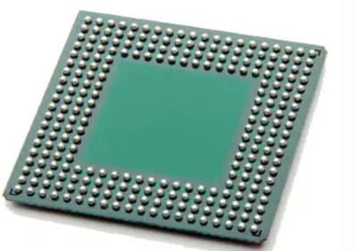
Ball Grid Array (BGA) is a type of surface mount packaging used for integrated circuits (ICs) and other semiconductor devices. It’s characterized by an array of solder balls arranged in a grid formation on the underside of the component. These solder balls serve as the connection points to the PCB.
However, working with BGAs requires specialized equipment and techniques for both assembly and rework due to the complexity of soldering the numerous small solder balls. Nonetheless, they are widely used in various applications, especially in high-performance computing, gaming consoles, networking hardware, and consumer electronics, where space and performance are critical considerations.
4. Chip Scale Packaging (CSP)
Chip Scale Packaging (CSP): mCSP (micro Chip Scale Package), WLP (Wafer-Level Package), FC-CSP (Flip Chip Chip Scale Package), etc.
Chip Scale Packaging (CSP) refers to a packaging technology for integrated circuits (ICs) where the package size closely matches the dimensions of the silicon die or chip itself. In essence, CSPs aim to minimize the footprint of the package while providing the necessary protection and connections for the chip.
CSPs are commonly used in portable electronic devices such as smartphones, tablets, wearables, and other miniaturized gadgets. Their small form factor and efficient use of space make them ideal for applications demanding high-performance chips in constrained areas.
5. Quad Flat Packages (QFP)
Quad Flat Packages (QFP): TQFP (Thin Quad Flat Package), PQFP (Plastic Quad Flat Package), LQFP (Low-profile Quad Flat Package), etc.
Quad Flat Packages (QFP) are a type of surface mount integrated circuit package characterized by a flat body and leads extending from all four sides of the component. The leads are arranged in a grid pattern, allowing for easy soldering to the printed circuit board (PCB).
QFPs were a popular choice for integrating moderate-to-high pin counts in a compact form factor before more miniaturized packages, such as Ball Grid Arrays (BGAs) and Chip Scale Packages (CSPs), gained prominence in the electronics industry.
6. Plastic Leaded Chip Carrier (PLCC)
Plastic Leaded Chip Carrier (PLCC): PQFP (Plastic Quad Flat Package), LQFP (Low-profile Quad Flat Package), etc.
A Plastic Leaded Chip Carrier (PLCC) is a type of integrated circuit (IC) package used for surface-mounted devices. It’s a square or rectangular package made of plastic with metal leads extending from the sides. PLCC packages typically contain a semiconductor chip and have leads or pins on all four sides, which are used for connection to a circuit board.
PLCCs have largely been replaced by smaller and more efficient packages like quad flat no-leads (QFN) and ball grid arrays (BGAs) in many modern electronic devices due to their higher pin density, smaller footprint, and improved electrical performance.
7. Transistor Outline (TO) Packages
Transistor Outline (TO) Packages: TO-92, TO-220, TO-263, TO-220AB, etc.
Transistor Outline (TO) packages are a standardized type of packaging used for discrete semiconductor components like transistors and some integrated circuits. These packages are designed to provide a standardized form factor for easy handling, mounting, and heat dissipation.
The TO packages are convenient for manual or automated assembly onto circuit boards, and their standardized dimensions make them easily interchangeable in various electronic designs. However, due to advancements in technology, smaller and more efficient packages like surface-mount devices (SMDs) are becoming more prevalent in modern electronic designs, reducing the use of TO packages in some applications.
8. Dual Flat No-Lead (DFN) Packages
Dual Flat No-Lead (DFN) Packages: WDFN (Thin Dual Flat No-Lead), SON (Small Outline No-Lead), QFN (Quad Flat No-Lead), etc.
Dual Flat No-Lead (DFN) packages are a type of surface-mount semiconductor package used for integrated circuits (ICs), such as microcontrollers, integrated power devices, and sensors. The DFN package is characterized by its small size, low profile, and absence of leads or pins extending from the package sides.
DFN packages have a flat bottom with exposed metal pads arranged in a grid pattern. The electrical connections are made by soldering these pads directly onto corresponding pads on the surface of a printed circuit board (PCB). The absence of leads makes DFN packages suitable for high-density mounting, as they occupy less space and offer improved electrical performance due to shorter interconnection paths.
DFN packages are popular in modern electronic devices where miniaturization and efficient use of space are crucial design considerations. Their compact size, good thermal performance, and ability to accommodate higher pin counts make them favored choices in many consumer electronics, telecommunications, and portable devices.
9. Small Outline Package (SOP)
Small Outline Package (SOP): TSOP (Thin Small Outline Package), SSOP (Shrink Small Outline Package), HSOP (Heatsink Small Outline Package), etc.
The Small Outline Package (SOP) is a type of surface-mount technology used for integrated circuits. SOP packages are characterized by their rectangular shape with gull-wing or “J”-bend leads extending from the sides.
These packages come in different variants, such as SOP, SOP-8, SOP-16, etc., indicating the number of leads (pins) present on the package. For instance, SOP-8 has 8 leads, while SOP-16 has 16 leads.
SOP packages were popular in the 1980s and 1990s and remain in use for various applications, including memory chips, microcontrollers, and other ICs. They were widely adopted due to their ease of handling, small size, and compatibility with automated assembly processes.
The gull-wing leads of SOP packages make them suitable for mounting onto the surface of a printed circuit board (PCB), allowing for more efficient use of board space and facilitating high-density mounting. The leads are usually spaced in a standardized pattern to ensure compatibility and ease of design across different manufacturers.
10. Dual In-Line Package (DIP)
Dual In-Line Package (DIP): PDIP (Plastic Dual In-line Package), CDIP (Ceramic Dual In-line Package), etc.
The Dual In-Line Package (DIP) is a type of electronic component package used primarily for integrated circuits (ICs) and other similar semiconductor devices. DIPs were widely used in the earlier days of electronics and computing but have become less common with advancements in surface-mount technology.
DIPs were prevalent in early computers, microcontrollers, memory chips, and other integrated circuits. However, as technology progressed, smaller and more efficient surface-mount packages like quad flat packages (QFP), small outline packages (SOP), and ball grid arrays (BGAs) gained popularity due to their smaller footprint, higher pin density, and better electrical performance.
11. Chip on Board (COB)
Chip on Board (COB): The semiconductor chip is mounted directly onto the PCB.
Chip on Board (COB) refers to a packaging technology in which semiconductor chips are mounted directly onto a substrate or circuit board and then covered with a protective layer of epoxy resin or other encapsulation materials. Instead of using traditional individual packages for each chip, COB involves placing bare semiconductor chips directly onto the substrate and connecting them through wire bonding or flip-chip bonding techniques.
COB technology finds applications in various electronic devices, including LED lighting, RFID tags, sensor modules, and certain types of microcontrollers. Its advantages in size, cost, and durability make it suitable for specific applications where space constraints and reliability are critical factors.
12. Metal Can Packages
Metal Can Packages: TO-CAN, FET CAN, etc.
Metal can packages refer to a type of packaging used for semiconductor devices, particularly in the early days of integrated circuits and discrete electronic components. These packages are made of metal and are designed to protect the semiconductor chip or component from environmental factors and provide mechanical stability.
Metal can packages were widely used in the past for diodes, transistors, operational amplifiers, and other electronic components. However, with advancements in semiconductor packaging technology, newer packaging formats like surface-mount packages (SMDs), plastic packages, and ceramic packages have become more prevalent due to their smaller size, lighter weight, and better thermal performance.
Despite their declining use in modern electronics, metal can packages are still employed in specialized applications where their specific properties, such as hermetic sealing or high-reliability requirements, are crucial, such as in certain military, aerospace, or high-reliability industrial applications.
13. Flip Chip
Flip Chip: The die is flipped onto the substrate and bonded without packaging.
Flip chip is an advanced packaging technique used in semiconductor manufacturing where the active surface of a microchip is inverted and directly connected to the substrate or carrier using tiny solder bumps or metal bumps. Instead of traditional wire bonding, where wires connect the chip to the substrate, flip chip technology directly attaches the active side of the chip to the carrier.
Flip chip technology is widely used in various applications, including microprocessors, memory chips, graphic processors, and high-performance integrated circuits found in computers, smartphones, networking devices, and other electronic devices. Its advantages in terms of performance, size, and reliability have made it a preferred packaging method in the semiconductor industry for many high-performance applications.
14. Wafer-Level Chip Scale Package (WLCSP)
Wafer-Level Chip Scale Package (WLCSP): Direct chip attachment on the wafer level.
Wafer-Level Chip Scale Package (WLCSP) is an advanced semiconductor packaging technology used to create extremely compact and miniaturized packages for integrated circuits (ICs). WLCSP is designed to minimize the package footprint, making it almost the same size as the actual semiconductor die, resulting in an ultra-small and thin package.
WLCSP technology involves the packaging process occurring directly on the wafer during the semiconductor manufacturing process. The individual ICs are packaged at the wafer level before they are separated into individual chips (dies). This approach reduces manufacturing steps and cost compared to traditional packaging methods.
WLCSPs are commonly used in various electronic devices where space savings, high performance, and miniaturization are essential, such as in mobile devices (smartphones, wearables), medical devices, and portable electronics.
15. Ceramic Packages
Ceramic Packages: Cerdip (Ceramic Dual In-line Package), CQFP (Ceramic Quad Flat Package), etc.
Ceramic packages are a type of semiconductor packaging made primarily from ceramic materials. These packages are used to encapsulate and protect integrated circuits (ICs), transistors, and other semiconductor devices.
Ceramic packages have been widely used in applications where high reliability, ruggedness, and thermal management are critical, such as in aerospace, automotive electronics, military applications, and certain industrial settings.
However, ceramic packaging tends to be more expensive compared to plastic or other materials, which has led to the development of alternative packaging technologies for consumer electronics. Nevertheless, for applications requiring superior thermal performance, reliability, and resilience to extreme conditions, ceramic packages remain a preferred choice.
16. Ceramic Ball Grid Array (CBGA)
Ceramic Ball Grid Array (CBGA): Ceramic package with a grid array of solder balls.
A Ceramic Ball Grid Array (CBGA) is a type of packaging used for integrated circuits (ICs) and semiconductor devices. It’s a variation of the ball grid array (BGA) packaging, where the package substrate is made of ceramic material instead of organic material (like fiberglass-reinforced epoxy resin).
CBGA packages are commonly used in applications that demand high reliability, ruggedness, and superior thermal management. These include aerospace, military, automotive, and certain industrial applications where extreme temperatures, mechanical stress, or harsh environments are encountered.
However, CBGA packages tend to be more expensive to manufacture compared to their organic substrate counterparts (like plastic BGAs), which has led to their more limited use in certain consumer electronics applications. Nevertheless, their exceptional thermal performance and reliability make them a preferred choice for specific high-end applications.
17. Hermetic Sealed Packages
Hermetic Sealed Packages: Complete seal for protection against environmental factors.
Hermetic sealed packages refer to electronic packaging that provides an airtight and moisture-proof enclosure for semiconductor devices, integrated circuits (ICs), sensors, or other sensitive electronic components. The term “hermetic” implies a complete seal that prevents the ingress of gases or moisture into the package.
Hermetic sealing ensures the long-term integrity and reliability of sensitive electronic components, especially in environments where exposure to moisture, gases, or contaminants could compromise their functionality. This level of protection is essential for maintaining the performance and longevity of electronic devices in demanding and critical applications.
18. Molded Packages
Molded Packages: Enclosed in a protective mold to shield against moisture and contaminants.
Molded packages, in the context of semiconductor manufacturing, refer to packaging technology where semiconductor devices or integrated circuits (ICs) are encapsulated within a molded plastic or resin material. This process involves molding the semiconductor chip and connecting wires within a protective casing made of plastic or resin.
These packages are not limited to a single type but encompass various packaging styles, such as Dual In-Line Packages (DIPs), Small Outline Packages (SOPs), Quad Flat Packages (QFPs), and many others. Molded plastic or resin packaging has been widely used due to its versatility, cost-effectiveness, and ability to meet the needs of various electronic applications.
19. Hybrid Packages
Hybrid Packages: Combines different packaging types into a single component.
Hybrid packages refer to semiconductor packaging that combines multiple semiconductor or electronic components in a single package, typically integrating different technologies or types of components onto a common substrate. These packages are called “hybrid” because they merge diverse technologies or functionalities within one enclosure.
The manufacturing of hybrid packages involves assembling different components onto a common substrate, which can be ceramic, organic, or other materials suitable for accommodating the diverse technologies being integrated. Assembly methods may involve wire bonding, die attach, flip chip bonding, or other advanced packaging techniques.
Hybrid packages offer a versatile solution for combining different electronic components to achieve desired functionalities, making them valuable in various industries where specific and specialized applications demand tailored solutions.
20. System-in-Package (SiP)
System-in-Package (SiP): Integrates multiple chips or devices into a single package.
System-in-Package (SiP) is an advanced packaging technology that integrates multiple chips, dies, or diverse components into a single package, forming a complete functional system. It differs from traditional multi-chip modules or single-chip ICs by combining various functionalities or entire subsystems into a compact and integrated package.
SiP technology finds applications in various fields, including mobile devices, Internet of Things (IoT) devices, wearables, telecommunications, automotive electronics, and more. Its ability to combine multiple functions or subsystems into a single package makes SiP an efficient and space-saving solution for complex electronic systems.
The manufacturing process for SiP involves assembling and interconnecting various chips or components onto a common substrate using advanced packaging techniques. Design considerations include thermal management, signal integrity, power distribution, and overall system optimization to ensure optimal performance of the integrated system.
Each of these packaging technologies serves specific purposes, balancing factors like size, performance, thermal management, and environmental protection for various electronic components and devices.
These packaging technologies, with their unique designs and functionalities, enable the creation of intricate electronic systems across diverse industries. Their evolution continues to meet the demands of miniaturization, performance enhancement, and innovation in modern electronics.
Online messageinquiry
- Week of hot material
- Material in short supply seckilling
| model | brand | Quote |
|---|---|---|
| MC33074DR2G | onsemi | |
| CDZVT2R20B | ROHM Semiconductor | |
| RB751G-40T2R | ROHM Semiconductor | |
| TL431ACLPR | Texas Instruments | |
| BD71847AMWV-E2 | ROHM Semiconductor |
| model | brand | To snap up |
|---|---|---|
| ESR03EZPJ151 | ROHM Semiconductor | |
| BU33JA2MNVX-CTL | ROHM Semiconductor | |
| BP3621 | ROHM Semiconductor | |
| IPZ40N04S5L4R8ATMA1 | Infineon Technologies | |
| STM32F429IGT6 | STMicroelectronics | |
| TPS63050YFFR | Texas Instruments |
- Week of ranking
- Month ranking
Qr code of ameya360 official account
Identify TWO-DIMENSIONAL code, you can pay attention to


Please enter the verification code in the image below:
