LED Packaging Companies Work on Niche Markets, Says TrendForce

发布时间:2019-01-24 00:00
作者:Ameya360
来源:TrendForce
阅读量:3775

  Mainstream high- and mid-power LED package products in the Chinese market witnessed price declines in December, according to the latest report from LEDinside, a division of TrendForce.

  “LED manufacturers have continued to clear their inventories in December due to the weak demand at the year end, which lowered the prices in the general lighting market”, says LEDinside analyst Terri Wang. The average prices of high- and mid-power LED package products slid 2%~4% and 1%~8% respectively.

  Faced with the sluggish demand, LED packaging companies continue to explore niche markets, with horticultural lighting, human centric lighting, and connected lighting being the focus. For instance, Lumileds has released the LUXEON SunPlus 2835 LED series for horticultural lighting, with eight color options and customized spectrum available. Samsung has also launched a new product series for horticultural lighting, including full-spectrum packages and modules. Blue light, red light, and infrared LEDs are available, and the products have been mass produced. For the future, Samsung plans to integrate smart sensing or connected solutions to horticultural lighting LED products. Nichia introduces COB, a new human centric lighting product series, which can be used for commercial lighting like retailing stores. The color temperature can change according to the features of products displayed, or according to users’ biological clock when used for home lighting.

(备注:文章来源于网络,信息仅供参考,不代表本网站观点,如有侵权请联系删除!)

在线留言询价

相关阅读
What is LED packaging?  Principles of LED packaging
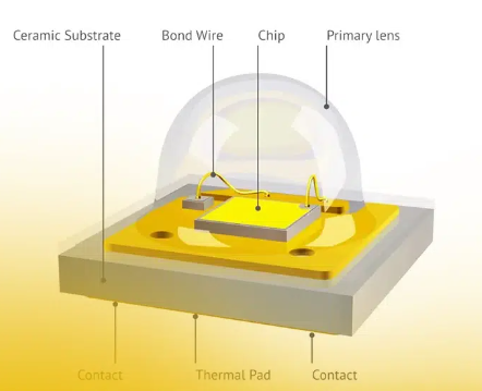
  LED packaging is an essential element in the world of lighting technology. It involves the process of encapsulating and protecting delicate LED components, allowing them to deliver high-performance illumination in a range of applications. With its compact size, energy efficiency, and long lifespan, LED packaging has revolutionized the way we illuminate our surroundings. In this article, we will talk about what is LED packaging, its importance, its principles, and general packaging methods.  What is LED packaging?  LED packaging refers to assembling LED chips and other components (such as connecting wires and packaging materials) together to form a complete LED lamp. The purpose of LED packaging is to enable the LED chip to work properly in practical applications and have sufficient brightness and stability.  Why is LED packaging needed?Generally speaking, the function of packaging is to protect the chip, extend the stability of the chip’s normal operation, and prevent the chip from being corroded by impurities in the air or mechanical damage from the outside and unable to continue to be used when exposed to the air for a long time. Specifically, the functions of LED packaging mainly include: 1. Mechanical protection to improve reliability; 2. Enhance heat dissipation to reduce chip junction temperature and improve LED performance; 3. Optical control to improve light extraction efficiency and optimize beam distribution; 4. Power supply management, including AC/DC conversion, power control, etc.  Principles of LED packagingThe principle of LED packaging can be divided into the following steps:  1. Preparation of LED chips: LED chips are the core components of LED lights and need to be prepared through chemical reactions and physical techniques. LED chips are usually made of two materials: n-type semiconductor and p-type semiconductor. The two materials form a PN junction through a chemical reaction. When a voltage is applied through the LED’s connecting wire, electrons and holes combine in the PN junction and generate photons, thereby emitting light.  2. Install electrodes and connecting wires: LED chips need to be installed with electrodes and connecting wires in order to transmit electrical signals to the chip. The electrodes and connecting wires are usually made of metal and can be fixed to the chip by soldering or bonding.  3. Packaging materials: Packaging materials are the key to combining LED chips and other components. Packaging materials usually have good waterproof properties, insulation properties and high temperature resistance. The packaging material can be materials such as plastic, glass or ceramic. The selection of packaging materials needs to be determined based on the purpose and application environment of the LED lamp.  4. Packaging process: The packaging process is to assemble the LED chip and other components together to form a complete LED lamp. The packaging process usually includes the following steps: placing the LED chip in the packaging material, fixing the electrodes and connecting wires, pouring the packaging material, heating and curing the packaging material. During the packaging process, attention needs to be paid to the uniformity and thickness of the packaging material to ensure the brightness and stability of the LED light.  To sum up, LED packaging is the process of combining LED chips and other components to form a complete LED lamp. The principle of LED packaging includes steps such as preparing LED chips, installing electrodes and connecting wires, packaging materials and packaging processes. Through scientific and reasonable packaging design and manufacturing technology, high-quality, high-brightness, and high-stability LED lights can be obtained.  What are the general packaging methods?The selection of LED packaging methods, materials, structures and processes is mainly determined by factors such as chip structure, optoelectronic/mechanical characteristics, specific applications and costs. After more than 40 years of development, LED packaging has successively gone through development stages such as Lamp LED, SMD LED, and Power LED. With the increase in chip power, especially the demand for the development of solid-state lighting technology, new and higher requirements have been put forward for the optical, thermal, electrical and mechanical structures of LED packages. In order to effectively reduce the thermal resistance of the package and improve the light extraction efficiency, new technical ideas must be adopted for package design.  After more than 40 years of development, LED packaging technology and structure have gone through four stages.  1. Pin-type (Lamp) LED packaging  The pin-type package is the commonly used A3-5mm package structure. Generally used for LED packages with smaller current (20-30mA) and lower power (less than 0.1W). It is mainly used for instrument display or indication, and can also be used as a display screen during large-scale integration. The disadvantage is that the package thermal resistance is large (generally higher than 100K/W) and the life is short.  2. Surface assembly (SMT-LED) packaging  Surface mounting technology (SMT) is a packaging technology that can directly attach and solder packaged devices to designated positions on the PCB surface. Specifically, specific tools or equipment are used to align the chip pins on the pad pattern that has been pre-coated with adhesive and solder paste, and then directly mounted on the PCB surface without drilling mounting holes, and then undergo wave soldering. Or after reflow soldering, a reliable mechanical and electrical connection is established between the device and the circuit. SMT technology has the advantages of high reliability, good high-frequency characteristics, and easy automation. It is the most popular packaging technology and process in the electronics industry.  3. Chip-on-board (COB) LED packaging  COB is the abbreviation of Chip On Board. It is a packaging technology that directly pastes the LED chip onto the PCB board through adhesive or solder, and then realizes the electrical interconnection between the chip and the PCB board through wire bonding. The PCB board can be made of low-cost FR-4 material (glass fiber reinforced epoxy resin), or it can be a metal-based or ceramic-based composite material with high thermal conductivity (such as an aluminum substrate or copper-clad ceramic substrate, etc.). Wire bonding can use thermosonic bonding at high temperatures (gold wire ball bonding) and ultrasonic bonding at room temperature (aluminum cleaver welding). COB technology is mainly used for LED packaging of high-power multi-chip arrays. Compared with SMT, it not only greatly improves the packaging power density, but also reduces the packaging thermal resistance (generally 6-12W/mK).  4. System in package (SiP) LED packaging  SiP (System in Package) is a new packaging integration method developed on the basis of System on Chip (SOC) in recent years to adapt to the portable development and miniaturization requirements of the entire machine. For SiP-LED, not only can multiple light-emitting wafers be assembled in one package, but also various types of devices (such as power supplies, control circuits, optical microstructures, sensors, etc.) can be integrated together to build a more complex and complete system. Compared with other packaging structures, SiP has good process compatibility (existing electronic packaging materials and processes can be used), high integration, low cost, can provide more new functions, is easy to be tested in blocks, and has a short development cycle. Etc. According to different technology types, SiP can be divided into four types: chip stack type, module type, MCM type and three-dimensional (3D) packaging type.
2023-10-16 13:38 阅读量:1849
AMEYA360:NanoLED Research Exploits Northern Roots
  NS Nanotech’s recent opening of a research and development center in Montreal represents a homecoming of sorts, as the company’s technology is based on research conducted at McGill University.  NS Nanotech Canada will take advantage of exclusive licenses to a portfolio of groundbreaking patents owned by McGill as part of its advanced research efforts to support commercialization of next-generation nanoLED technologies for televisions, mobile phones, smartwatches, augmented-reality headsets and other applications, the company said in prepared remarks.  In an interview with EE Times, NS Nanotech CEO Seth Coe-Sullivan said the R&D center is a critical enablement of the company’s long-term mission to develop the world’s first efficient submicron-scale nanoLEDs.  NS Nanotech, which is based in Ann Arbor, Michigan, has created samples of submicron-sized LEDs in its laboratory research that are radically smaller than any other LEDs available in the world today—these submicron nanoLEDs are much smaller than a strand of human hair, at less than one micron. By comparison, today’s “miniLEDs” are generally between 100 and 200 microns, while new “microLEDs” are smaller than 100 microns.Coe-Sullivan said McGill is a global center of excellence in nanotechnologies that will help NS Nanotech overcome the cost and performance limitations of 20th century technologies.  The McGill University campus in Montreal (Source: Neale McDevitt/McGill University)  “What happens to conventional technology is you make the LED smaller, and the efficiency gets smaller as well,” he said. “That’s where a nanoLED comes in.” By building the LED from the nano up, no efficiency is lost. “The efficiency versus size curve is very favorable.”  NS Nanotech’s strategy since its founding was to be “capital light,” despite being in the capital-intensive semiconductor industry, Coe-Sullivan said. “Raising a lot of capital is great. You get to buy a lot of shiny new toys.” But as much as engineers love their toys, he added, it’s not desirable from a financial point of view. “It’s a big hole to be digging yourself.”  By collaborating with universities like McGill and the University of Michigan, NS Nanotech can send its engineers to the necessary equipment, such as a molecular beam epitaxy (MBE) chamber, rather than making huge capital investments, Coe-Sullivan said. “We scoured the world for that.”  The company was already a licensee of McGill IP and technology, which meant it already had a formal relationship with the university and its technology transfer office.  Derrick Wong, COO of NS Nanotech, played a key role in the original technology transfer license. It’s fitting that he’s back in the picture at NS Nanotech after retiring from McGill, as he knows many of the people at NS Nanotech. This includes some who are repatriating back to Canada for the R&D center, such as senior research scientist David Laleyan, a McGill graduate who received his Ph.D. from the University of Michigan in 2020.  David Laleyan, senior scientist at NS Nanotech Canada (left); Derrick Wong, COO of NS Nanotech Canada (center); and McGill University professor Songrui Zhao (right) work with nanoLED fabrication equipment at Professor Zhao’s research laboratory.  “Although we started this officially in November, people have been working together on this project in various forms for the last nine years,” Wong said in the same interview with EE Times. “McGill University has been very supportive. It still views NS Nanotech as a McGill startup, even though it’s located in Ann Arbor. It’s very much a McGill success story.”  Also collaborating with NS Nanotech is Songrui Zhao, assistant professor in the Department of Electrical and Computer Engineering at McGill University, whose research is contributing to solving the challenges related to nanoLEDs. Over the past few years, McGill has been working with MBE, which is a material growth technique to grow nanowires for very small-scale LEDs and lasers because nanowires provide better material quality, Zhao said in the same interview with Coe-Sullivan and Wong. “If you are using this molecular beam epitaxy technique to grow nanowires, it’s very, very unique, and there are not many players.”  Zhao added that a chief benefit of conducting this research in a university environment is that there’s a lot of frank interaction with students to discuss many different ideas. “We are not driven by revenue,” he said. University/industrial partnerships can accelerate the technology development and facilitate international connections. “One team cannot solve all the problems.”  While McGill can handle MBE, materials and even initial device development, Zhao said testing and scaling up requires more resources beyond the university—be it people or equipment.  Coe-Sullivan said the immediate goal is to grow the team in Montreal to work with the research equipment available there. “At McGill, we’ve got access to great research tools, but they’re research tools. These are not places where we’re ever going to mass-produce a product or be able to truly scale a technology.”  He said NS Nanotech is talking to foundries that have the same type of equipment, but at a much larger scale and throughput to be able to bring its product all the way to market through partnerships and contract manufacturing. “We’ve got access to foundries here in North America that can take this all the way to the end market.”  In late April, NS Nanotech Canada announced it received matching funding support from McGill University’s Office of Innovation & Partnerships to accelerate the commercialization of its nanoLED technologies.
2023-06-09 13:16 阅读量:1300
U.S. LED Light Bulb Prices Rose in September due to Trade War
Terri Wang, LEDinside analyst, points out that the scales of the price drop of high- and mid-power products varied in September, with those of the 0.2 W and 0.5 W 2835 LEDs reaching 2% and 3% on average, respectively. Meanwhile, prices of high power ceramic-substrate LEDs declined by 2-3%, as their shares in the markets of architectural, outdoor, and commercial lighting have been gradually taken over by 5050 LEDs. To further expand their market share, suppliers have been dedicated to increasing their products' added value and upgrading their performance. CREE, for example, has released the XLamp XP-G3 S Line LED suitable for connected lighting, and featuring more reliable cycling and dimming cycling performance, higher sulfur-resistance, and higher light output and luminescent efficiency than the standard XP-G3.On the automotive market, higher luminosity of high/low beams increases the scope of visibility and alleviates the problem of glare. ADB headlights have been introduced to the medium-tier auto market in 2018, such as the lateral eight-pixel solution which has been employed by Chinese auto brands.LED bulb prices experience slight growth on the global market; US prices to be impacted the most due to trade warIn September, the average retail price of 40W equivalent LED light bulbs rose by 1.2% to US$6.2, while that of 60W equivalent LED light bulbs inched up by 0.7% to US$7.3.Affected by trade war, branded LED light bulb suppliers in the U.S. have begun to raise prices to pass increased costs from higher tariffs to consumers, as a result of which the average retail prices of 40W and 60W equivalent LED light bulbs rose by 4.3% and 3.6%, respectively, in September. Another reason for the price hike was the return of higher-priced smart lighting products to the market. In Germany, the ban imposed on halogen light bulbs by the EU starting from September 1st of this year has spurred demands for LED light bulbs. This has caused the average retail prices for Germany’s 40W and 60W equivalent LED light bulbs to advance by 3.8% and 3.1%, respectively. The LED light bulb prices from the major brands, such as Osram and Philips, all rose during this period.As for the other markets, the prices of 40W and 60W equivalent LED light bulbs in Japan and China all dropped by 0.1-1.3%, while those in South Korea have remained stable. 
2018-10-12 00:00 阅读量:1257
Micro LED & Mini LED Market Expects Explosive Business Opportunities, with an Estimated Market Value of $1.38 Billion by 2022
Micro LED displays and Mini LED backlight technology have been the focus of spotlight in this year’s exhibitions of consumer electronics and display technology. Major manufacturers including Samsung, Sony, and AUO have showcased related conceptual products. It is also said that Samsung may mass-produce ultra-large Micro LED TVs, driving more manufacturers to invest in Mini LED R&D. According to the latest report of LEDinside, a division of TrendForce, the market value of Micro LED and Mini LED products is estimated at US$1.38 billion by 2022.New technologies will accelerate the advancement of Micro LED“Micro LED still faces many technical bottlenecks, including epitaxial wafer/chip, transfer, full color, driver IC, backplane and inspection/repair technology”, says Roger Chu, the Research Director of LEDinside. Transfer technology used to be the biggest bottleneck, but new transfer solutions have been emerging, such as Pick & Place transfer, fluid assembly, laser transfer, and roller transfer. It is expected that there will be more cost-competitive solutions in the future, which may accelerate the advancement of Micro LED.LEDinside notes that Micro LED technology is most likely adopted to display products with special requirements, especially those beyond the capabilities of LCD and OLED displays. LEDinside expects that Micro LED would be gradually applied to AR micro projections which require high brightness, automotive HUD projection applications, and ultra-large digital display in the near future. LEDinside estimates that the market value of Micro LED products will reach US$694 million by 2022.Mini LED expects growing demand in high-end backlight marketConsidering existing technical barriers for Micro LED technology, manufacturers tend to launch Mini LED backlight solutions this year, hoping to boost the demand. Displays using Mini LED backlight may appear in the market in the second half of 2018, says LEDinside, and the market value of Mini LED products is expected to reach US$689 million by 2022.Different from conventional LED backlight, Mini LED chips are smaller in size. Coupled with direct type LED backlight and local dimming, the number of LED chips used will grow at multiples. Therefore, Mini LED will become a key application that drives the demand for LED chips.However, the costs of Mini LED backlight remain too high for mainstream displays, while problems of heat dissipation and power consumption have not been solved yet. Therefore, Mini LED may cut into the market through high-end consumer products like gaming notebook, gaming monitors, monitor with special applications, as well as niche products like high-end TV with high resolution, high contrast and high color saturation. These products put more focus on specifications than on competitive prices, thus will become the main battlefield for vendors who aim to achieve technology differentiation through Mini LED backlight technology.
2018-06-22 00:00 阅读量:1485
  • 一周热料
  • 紧缺物料秒杀
型号 品牌 询价
TL431ACLPR Texas Instruments
RB751G-40T2R ROHM Semiconductor
MC33074DR2G onsemi
BD71847AMWV-E2 ROHM Semiconductor
CDZVT2R20B ROHM Semiconductor
型号 品牌 抢购
TPS63050YFFR Texas Instruments
BU33JA2MNVX-CTL ROHM Semiconductor
BP3621 ROHM Semiconductor
ESR03EZPJ151 ROHM Semiconductor
IPZ40N04S5L4R8ATMA1 Infineon Technologies
STM32F429IGT6 STMicroelectronics
热门标签
ROHM
Aavid
Averlogic
开发板
SUSUMU
NXP
PCB
传感器
半导体
相关百科
关于我们
AMEYA360微信服务号 AMEYA360微信服务号
AMEYA360商城(www.ameya360.com)上线于2011年,现 有超过3500家优质供应商,收录600万种产品型号数据,100 多万种元器件库存可供选购,产品覆盖MCU+存储器+电源芯 片+IGBT+MOS管+运放+射频蓝牙+传感器+电阻电容电感+ 连接器等多个领域,平台主营业务涵盖电子元器件现货销售、 BOM配单及提供产品配套资料等,为广大客户提供一站式购 销服务。