STMicroelectronics to Invest EUR 5 Billion in New SiC Wafer Fab

发布时间:2023-11-30 10:53
作者:AMEYA360
来源:trendforce
阅读量:2168

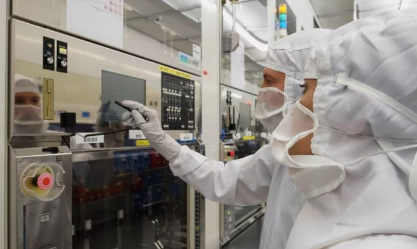
  STMicroelectronics, following its EUR 7.5 billion wafer fab project with GlobalFoundries in Crolles, France. is set to invest EUR 5 billion in building a new SiC super semiconductor wafer fab in Catania, Sicily, Italy. The fab in Italy will specialize in producing SiC chips, a pivotal technology for electric vehicles with substantial growth potential, according to French media L’Usine Nouvelle on November 26th,
STMicroelectronics to Invest EUR 5 Billion in New SiC Wafer Fab

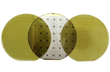
  STMicroelectronics competitively plans to transition to 8-inch wafers starting from 2024. The company will integrate Soitec’s SmartSiC technology to enhance efficiency and reduce carbon emissions. Simultaneously, STMicroelectronics aims to increase capacity, achieve internal manufacturing, and collaborate with Chinese firm Sanan Optoelectronics to raise SiC chip-related revenue from the expected USD 1.2 billion in 2023 to USD 5 billion by 2030.

  On June 7th earlier this year, STMicroelectronics and Sanan Optoelectronics announced a joint venture to establish a new 8-inch SiC device fab in Chongqing, China, with an anticipated total investment of USD 3.2 billion.

  To ensure the successful implementation of this extensive investment plan, Sanan Optoelectronics said to utilize its self-developed SiC substrate process to construct and operate a new 8-inch SiC substrate fab independently.

  TrendForce: over 90% SiC market share by major global players

  According to TrendForce, the SiC industry is currently dominated by 6-inch substrates, holding up to 80% market share, while 8-inch substrates only account for 1%. Transitioning to larger 8-inch substrates is a key strategy for further reducing SiC device costs.

  8-inch SiC substrates offer significant cost advantages than 6-inch substrates. The industry’s major players in China, including SEMISiC, Jingsheng Mechanical & Electrical Co., Ltd. (JSG), Summit Crystal, Synlight Semiconductor, KY Semiconductor, and IV-SemiteC, are advancing the development of 8-inch SiC substrates. This shift from the approximately 45% of total production costs associated with substrates is expected to facilitate the broader adoption of SiC devices and create a positive cycle for major companies.

  Not only Chinese companies but also international semiconductor giants like Infineon Technologies and Onsemi are actively vying for a share of the market. Infineon has already prepared the first batch of 8-inch wafer samples in its fab and plans to convert them into electronic samples soon, with mass production applications scheduled before 2030. International device companies like Onsemi and ROHM have also outlined development plans for 8-inch SiC wafers.

  Currently, major companies hold over 90% of the market share, intensifying competition. A slowdown in progress could provide opportunities for followers. According to TrendForce, the market share of the top 5 SiC power semiconductor players in 2022 was dominated by STMicroelectronics (36.5%), Infineon (17.9%), Wolfspeed (16.3%), Onsemi (11.6%), and ROHM (8.1%), leaving the remaining companies with only 9.6%.

(备注:文章来源于网络,信息仅供参考,不代表本网站观点,如有侵权请联系删除!)

在线留言询价

相关阅读
STMicroelectronics Automotive-grade Devices Feature Enhanced Power Densities
  STMicroelectronics has introduced five power-semiconductor bridges in popular configurations, housed in its advanced ACEPACK SMIT package that eases assembly and enhances power density over conventional TO-style packages.  Engineers can choose from two STPOWER 650V MOSFET half bridges, a 600V ultrafast diode bridge, a 1.2kV half-controlled full-wave rectifier, and a 1.2kV thyristor-controlled bridge leg. All devices meet automotive-industry requirements and are suitable for electric vehicle on-board chargers (OBC) and DC/DC converters, as well as industrial power conversion.  ST’s ACEPACK SMIT surface mounted package delivers the easy handling of an insulated package with the thermal efficiency of an exposed drain. It allows direct-bonded copper (DBC) die attachment for efficient top-side cooling. The 4.6cm2 exposed metal topside of the ACEPACK SMIT permits easy attachment of a planar heatsink. This creates a space-saving low profile that maximizes thermal dissipation for greater reliability at high power. The module and heatsink can be placed using automated inline equipment, which saves manual processes and boosts productivity.  While minimizing the stack height and enhancing power density, the topside cooling design and 32.7-by-22.5mm package footprint allow 6.6mm lead-to-lead creepage distance. The tab-to-lead insulation is 4.5kVrms. The package also has low parasitic inductance and capacitance.  The SH68N65DM6AG and SH32N65DM6AG 650V-MDmesh DM6 MOSFET half bridges now available in ACEPACK SMIT are AQG-324 qualified. Their Rds(on) (max) of 41m? in the SH68N65DM6AG and 97m? in the SH32N65DM6AG ensures high electrical efficiency and low thermal dissipation. They can be used in DC/DC converters for both OBC and high voltage to low voltage section. Their multi-role flexibility helps streamline inventory and simplify procurement.  The STTH60RQ06-M2Y 600V, 60A full-wave bridge rectifier comprises ultrafast diodes with soft recovery characteristic and is PPAP capable for use in automotive applications.  The STTD6050H-12M2Y 1.2kV, 60A half-controlled single-phase AC/DC bridge rectifier is AEC-Q101 qualified and has high noise immunity with dV/dt of 1kV/μs.  The STTN6050H-12M1Y is a 1.2kV, 60A half bridge that comprises two internally connected thyristors (silicon-controlled rectifiers – SCRs). AEC-Q101 qualified, it can be used in automotive OBCs and charging stations and industrial applications such as AC/DC conversion in motor drives and power supplies, single- and tri-phase controlled rectifier bridges, totem-pole power-factor correction, and solid-state relay.
2023-01-12 10:43 阅读量:3359
Embedded AI Solutions Ease ML Development
  STMicroelectronics has released upgrades to both NanoEdge AI Studio and STM32Cube.AI to accelerate embedded artificial intelligence (AI) and machine learning (ML) development projects. These tools facilitate moving AI and ML to the edge of an application. At the edge, AI/ML delivers substantial advantages, which include privacy by design, deterministic and real-time response, greater reliability, and lower power consumption.  NanoEdge AI Studio is an automated ML tool for applications that do not require the development of neural networks. It is used with STM32 microcontrollers (MCUs) and MEMS sensors that include ST’s unique embedded intelligent sensor processing unit (ISPU). For developers needing to use neural networks, STM32Cube.AI is an AI model optimizer and compiler for STM32. The two new releases deliver features that help design and implement high-performance AI/ML solutions quickly and with minimum investment.  NanoEdge AI Studio version 3.2 now contains an automatic datalogger generator that increases development productivity. Its inputs include the ST development board and developer-defined sensor parameters, such as data rate, range, sample size, and number of axes. With these, NanoEdge AI Studio produces the binary for the development board without the developer having to write any code.  Because dataset quality directly impacts machine learning performance, the new data-manipulation features in NanoEdge AI Studio allow the user to clean and optimize the captured data in the NanoEdge AI Studio in a few clicks. A new validation stage has also been added, which helps users assess their algorithms by showing inference time, memory usage, and common performance metrics such as the accuracy, and F1-Score. It also highlights more information about the pre-processing and ML model involved in the selected library. The newest enhancement to the NanoEdge AI Studio adds more pre-processing techniques and ML models for anomaly detection and regression algorithms that boost performance. In addition, the tool supports creation of smart libraries that can predict future system states using multi-order regression models.  STM32Cube.AI version 7.3 is an essential tool for developing cutting-edge AI/ML solutions. Fully integrated into the STM32 ecosystem, it enables conversion of pretrained neural networks into optimized C code for the industry’s most popular family of 32-bit Arm? Cortex?-core MCUs. The enhanced STM32Cube.AI adds greater flexibility for neural-network (NN) optimizations. The tool can adapt existing neural networks to achieve performance demands, fit within memory limitations, or, in a balanced optimization, get the best of both. The update also brings support for TensorFlow 2.10 models and new kernel performance improvements.
2023-01-09 10:51 阅读量:3331
STMicroelectronics and eYs3D Microelectronics to Highlight 3D Stereo-vision Camera at CES 2023
  STMicroelectronics and eYs3D Microelectronics will showcase the results of their collaboration on high-quality machine vision at CES 2023 in Las Vegas on January 5-8. Using live demonstrations, the companies will highlight how stereo video and depth camera made from advanced active-coded infrared technology can enhance capabilities like feature recognition and autonomous guidance at mid-to-long working range.  “STMicroelectronics’ advanced image sensors, using proprietary process technologies, offer class-leading pixel size while offering both high sensitivity and low crosstalk,” said James Wang, Chief Strategy & Sales Officer, eYs3D Microelectronics. “Such high-performance image sensors at a competitive price point enable us to achieve extremely compact system size while ensuring outstanding machine-vision performance. The strong connection we have established with ST increases our confidence to develop new products that will lead the machine vision market.”  “The collaboration with eYs3D Microelectronics, through their expertise in capture, perception understanding, and 3D-fusion, offers ST additional business opportunities, use cases, and ecosystems addressing demands for stereo vision in applications such as robots, home-automation, home appliances, and many others,” said David Maucotel, Business Line Manager at ST’s Imaging Sub-Group. “While the reference designs showcased at CES are using monochromatic sensors, we can already foresee exciting enhancements and further use-cases using the RGB and RGB-IR versions of our sensors.”  The CES demonstrations highlight two jointly developed reference designs, the Ref-B6 and Ref-B3 ASV (Active Stereo Vision) video and depth cameras. Both combine the eYs3D CV processor and eSP876 stereo 3D Depth-Map chipset with ST’s global shutter image sensors that provide enhanced near-infrared (NIR) sensitivity. The embedded eYs3D chipset enhances object edge detection, optimizes depth de-noising, and outputs HD-quality 3D depth data up to 60 fps frame rate. ST’s image sensors enable the cameras to output data streams in various combinations of video/depth resolution and frame rate for the best quality depth sensing and point-cloud creation.  In addition, optimized lenses, filters and a VCSEL active-IR projector source optimize the infrared optical path and maximize immunity to ambient light noise. A specially developed control algorithm turns the IR projector on and o? alternately to permit capturing artifact-free gray scale images. Leveraging this advanced hardware design, the Ref-B6 stereo-video camera achieves a 6-centimeter baseline and 85deg(H) x 70deg(V) depth field of view.
2023-01-05 13:02 阅读量:3124
STMicroelectronics and Soitec Partner on SiC Substrate Manufacturing Technology
  The goal of the cooperation is the adoption by ST of Soitec's SmartSiC technology for its future 200mm substrate manufacturing.  STMicroelectronics and Soitec have announced the next stage of their cooperation on silicon carbide (SiC) substrates, with the qualification of Soitec’s SiC substrate technology by ST planned over the next 18 months. The goal of this cooperation is ST’s adoption of Soitec’s SmartSiC technology for its future 200mm substrate manufacturing, feeding its devices and modules manufacturing business, with volume production expected in the midterm.  “The transition to 200mm SiC wafers will bring substantial advantages to our automotive and industrial customers as they accelerate the transition toward electrification of their systems and products. It is important in driving economies of scale as product volumes ramp,” said Marco Monti, President Automotive and Discrete Group, STMicroelectronics. “We have chosen a vertically integrated model to maximize our know-how across the full manufacturing chain, from high-quality substrates to large-scale front- and back-end production. The goal of the technology cooperation with Soitec is to continue to improve our manufacturing yields and quality.”  “The automotive industry is facing major disruption with the advent of electric vehicles. Our cutting-edge SmartSiC technology, which adapts our unique SmartCut™ process to silicon carbide semiconductors, will play a key role in accelerating their adoption,” said Bernard Aspar, Chief Operating Officer of Soitec. “The combination of Soitec’s SmartSiC™ substrates with STMicroelectronics’ industry-leading silicon carbide technology and expertise is a game-changer for automotive chip manufacturing that will set new standards.”  SiC is a disruptive compound semiconductor material with intrinsic properties providing superior performance and efficiency over silicon in key, high-growth power applications for electric mobility and industrial processes, among others. It allows for more efficient power conversion, lighter and more compact designs, and overall system-design cost savings – all key parameters and factors for success in automotive and industrial systems. Transitioning from 150mm to 200mm wafers will enable a substantial capacity increase, with almost twice the useful area for manufacturing integrated circuits, delivering 1.8 – 1.9 times as many working chips per wafer.  SmartSi™ is a proprietary Soitec technology which uses Soitec proprietary SmartCut™ technology, to split a thin layer of a high quality SiC ‘donor’ wafer, and bond it on top of a low resistivity ‘handle’ polySiC wafer. The engineered substrate then improves device performance and manufacturing yields. The prime quality SiC ‘donor’ wafer can be reused multiple times, significantly reducing the overall energy consumption required to produce it.
2023-01-04 09:37 阅读量:1805
  • 一周热料
  • 紧缺物料秒杀
型号 品牌 询价
BD71847AMWV-E2 ROHM Semiconductor
RB751G-40T2R ROHM Semiconductor
TL431ACLPR Texas Instruments
MC33074DR2G onsemi
CDZVT2R20B ROHM Semiconductor
型号 品牌 抢购
IPZ40N04S5L4R8ATMA1 Infineon Technologies
TPS63050YFFR Texas Instruments
ESR03EZPJ151 ROHM Semiconductor
STM32F429IGT6 STMicroelectronics
BU33JA2MNVX-CTL ROHM Semiconductor
BP3621 ROHM Semiconductor
热门标签
ROHM
Aavid
Averlogic
开发板
SUSUMU
NXP
PCB
传感器
半导体
相关百科
关于我们
AMEYA360微信服务号 AMEYA360微信服务号
AMEYA360商城(www.ameya360.com)上线于2011年,现 有超过3500家优质供应商,收录600万种产品型号数据,100 多万种元器件库存可供选购,产品覆盖MCU+存储器+电源芯 片+IGBT+MOS管+运放+射频蓝牙+传感器+电阻电容电感+ 连接器等多个领域,平台主营业务涵盖电子元器件现货销售、 BOM配单及提供产品配套资料等,为广大客户提供一站式购 销服务。