What is the difference between thick film and thin film circuit board?

发布时间:2023-12-04 17:55
作者:AMEYA360
来源:AMEYA360
阅读量:1334

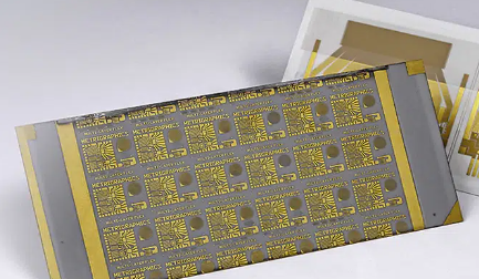
  Thin film circuit boards are specialized substrates used in electronic applications where precision, miniaturization, and high performance are crucial. They’re constructed by depositing thin layers of conductive, resistive, or insulating materials onto a substrate, typically made of ceramic or glass.
What is the difference between thick film and thin film circuit board?

  What is a thick film circuit board?A thick film circuit board refers to a type of printed circuit board (PCB) that utilizes thick film technology in its manufacturing process. In contrast to traditional thin film PCBs, which use thin layers of conductive material deposited on the board, thick film circuit boards involve the deposition of thicker layers of conductive and resistive materials on the board’s surface.

  The manufacturing process involves screen printing a paste-like mixture of conductive materials, such as silver, gold, or palladium, along with glass or ceramic materials, onto the substrate. This thick film paste is then fired at high temperatures to fuse the materials onto the board, forming the conductive traces, resistors, and other circuit elements.Thick film circuit boards offer several advantages:

  Cost-Effectiveness: The manufacturing process is generally less expensive compared to traditional thin film technologies.

  Ease of Prototyping: Thick film technology allows for rapid prototyping and quick modifications to circuit designs.

  Adaptability: They are suitable for hybrid circuits, combining both passive and active components on the same substrate.

  Robustness: Thick film boards tend to be more durable and resistant to environmental factors like moisture and temperature variations.

  These boards find applications in various industries, including automotive electronics, industrial controls, sensors, and certain medical devices where cost-effective and robust circuitry is required.

  What is a thin film circuit board used for?Thin film circuit boards are primarily used in applications where high precision, high-frequency, and high-performance electronic circuits are necessary. These boards are manufactured by depositing thin layers of conductive materials, typically metals like gold, platinum, or alloys, onto a substrate using specialized deposition techniques such as sputtering or chemical vapor deposition.

  Some common applications of thin film circuit boards include:

  High-Frequency Electronics: Thin film boards excel in high-frequency applications such as microwave devices, satellite communication systems, and radar systems due to their low signal loss and high-frequency capabilities.

  Aerospace and Defense: These boards are extensively used in aerospace and defense applications where reliability, miniaturization, and high performance are critical, including in avionics, navigation systems, and military-grade electronics.

  Telecommunications: Thin film technology is employed in telecommunications equipment where high-speed data transmission and signal integrity are essential, such as in network infrastructure and data centers.

  Medical Devices: Certain medical devices, especially those requiring precise sensors or high-frequency components, use thin film circuitry for their compactness and reliability, such as in medical imaging devices or diagnostic equipment.

  Optoelectronics: Thin film boards are used in optoelectronic devices like LEDs, photodetectors, and fiber optics due to their compatibility with optical materials and precise fabrication requirements.

  Consumer Electronics: In some specialized consumer electronics requiring high performance, like certain types of audio equipment or high-speed data processing devices, thin film technology might be employed.

  These applications benefit from the thin film’s precise deposition, allowing for highly accurate and controlled circuit elements, low noise, excellent signal integrity, and the ability to operate at high frequencies.

  What is the difference between thick film and thin film circuit board?The difference between thick film and thin film circuit boards primarily lies in their manufacturing processes, material thickness, and applications:

  Manufacturing Process:

  Thick Film: Thick film circuit boards are manufactured by depositing relatively thicker layers of conductive materials (usually pastes containing metal oxides) onto a substrate through screen printing or stencil printing processes. These layers are then fired or cured to create the circuitry.

  Thin Film: Thin film circuit boards are made by depositing very thin layers of conductive materials (typically metals like gold, platinum, or alloys) onto a substrate using advanced deposition techniques such as sputtering or chemical vapor deposition.

  Material Thickness:

  Thick Film: The conductive and insulating layers in thick film circuits are relatively thicker, often in the range of several micrometers to tens of micrometers.

  Thin Film: In contrast, thin film circuits have extremely thin conductive layers, typically in the range of a few nanometers to a few micrometers.

  Applications:

  Thick Film: Thick film circuits are commonly used in applications where cost-effectiveness, robustness, and moderate precision are required. They find use in automotive electronics, household appliances, sensors, and some medical devices.

  Thin Film: Thin film circuits excel in applications that demand high precision, high frequency, low noise, and superior performance. They are used in high-frequency communication systems, aerospace technology, defense applications, and high-end electronic devices where miniaturization and precision are critical.

  Performance:

  Thick Film: These circuits typically have higher resistance and lower precision compared to thin film circuits.

  Thin Film: Thin film circuits offer higher precision, low signal loss, excellent high-frequency performance, and are capable of handling high-speed data transmission due to their minimal thickness and precise fabrication.

  In summary, thick film and thin film circuit boards differ in their manufacturing techniques, material thickness, and the applications they are best suited for.

(备注:文章来源于网络,信息仅供参考,不代表本网站观点,如有侵权请联系删除!)

在线留言询价

相关阅读
Choke Inductors What They Are and What They Do
  Have you ever wondered how your phone stays charged or how your car radio delivers crystal-clear sound even on a bumpy road? The answer might lie in a tiny, unassuming component called a choke inductor. While they may not be the flashiest parts in your electronics, choke inductors are critical in ensuring smooth operation and clean power delivery across many devices. In this blog, we will look into the world of choke inductors and explain their function, work, and applications in everyday electronics.  What is a Choke Inductor?  A choke inductor, also commonly referred to as a choke coil inductor or simply a choke, is a passive electronic component that acts like a gatekeeper for electrical current. Unlike its cousin, the resistor, which dissipates energy as heat, a choke inductor manipulates the current flow based on its frequency. Here's the key difference:  Choke inductors: Block high-frequency alternating current (AC) while allowing direct current (DC) and lower-frequency AC to pass through.  Resistors: Resist all current frequencies, reducing the overall current flow and dissipating energy as heat.  This selective filtering property makes choke inductors essential components in various electronic circuits, ensuring clean power delivery and mitigating unwanted electrical noise.  How Does a Choke Inductor Work?  The magic behind choke inductors lies in their ability to generate a magnetic field when current flows through their coil. This magnetic field, in turn, opposes any changes in current. Here's a breakdown:  Current Flow: When current passes through the coil's wire, a magnetic field is generated around it.  Magnetic Field Opposition: According to Faraday's Law of electromagnetic induction, this magnetic field tries to resist changes in the current that created it.  Frequency Dependence: High-frequency AC signals involve rapid changes in the current direction. The opposing magnetic field substantially affects these rapid changes, making it more difficult for the high-frequency AC to pass through the choke.  DC and Low-Frequency AC: The changes in current are slower for direct current (DC) and lower-frequency AC. The opposing magnetic field has less impact, allowing these currents to pass through the choke with minimal hindrance.  Purpose of a Choke Inductor  Choke inductors offer a variety of functionalities in electronic circuits. Here are some of their essentialkey purposes:  Filtering: As mentioned, choke inductors filter out unwanted high-frequency noise from AC signals. This is crucial for ensuring clean power delivery and preventing interference with other components in the circuit.  Energy Storage: Choke inductors can store energy in their magnetic field when current flows through them. This stored energy can then be released back into the circuit when needed. This property is beneficial in circuits requiring power regulation or transient voltage suppression.  Voltage Regulation: Choke inductors can regulate circuit voltage levels with capacitors. By controlling the flow of current and the energy stored within the magnetic field, choke inductors help maintain a stable voltage output.  Types of Choke Inductors  While the basic operating principle remains the same, choke inductors come in various types based on their core material:  Air-Core Chokes: These chokes have an air core that offers low inductance (the ability to store energy magnetically) but works well at high frequencies. They are typically used in RF (radio frequency) circuits.  Iron-Core Chokes: Iron-core chokes provide higher inductance than air-core chokes, making them suitable for applications requiring more energy storage or filtering lower-frequency AC noise. However, they can suffer from core losses at higher frequencies.  Ferrite-Core Chokes: Ferrite is a ceramic material commonly used in choke inductors. It offers a good balance between inductance and core losses, making it a versatile choice for many applications, especially beneficial for high-frequency filtering applications.  Real-World Applications  Choke inductors are ubiquitous in various electronic devices:  Automotive Electronics: They play a vital role in power supplies for car audio systems, engine control units (ECUs), and other electronic components, filtering out noise and ensuring smooth operation.  Power Electronics: Choke inductors are essential in switch-mode power supplies, filtering out switching noise and regulating voltage for various electronic devices.  Radio Frequency (RF) Circuits: In RF circuits, choke inductors prevent unwanted signals from leaking out and interfering with other circuits. This ensures efficient signal transmission and reception.  Final Thoughts  Choke inductors are workhorses in electronics, silently ensuring clean power delivery, signal integrity, and protection from unwanted interference. By understanding their operating principles and various types, you gain valuable insight into the intricate workings of electronic circuits. Whether you're a seasoned engineer or an electronics enthusiast, appreciating the role of choke inductors empowers you to design and troubleshoot circuits more effectively.
2024-05-24 13:26 阅读量:735
Top 10 IC Design Houses’ Combined Revenue Grows 12% in 2023, NVIDIA Takes Lead for the First Time, Says TrendForce
  In 2023, the combined revenue of the world’s top ten IC design houses reached approximately $167.6 billion, marking a 12% annual increase. This growth was primarily driven by NVIDIA, which saw a remarkable 105% increase in revenue, significantly boosting the overall industry. While Broadcom, Will Semiconductor, and MPS experienced only marginal revenue growth, other companies faced declines due to economic downturns and inventory reductions, says TrendForce.  Looking ahead to 2024, TrendForce predicts that with IC inventory levels returning to healthy standards and driven by the AI boom, major CSPs will continue to expand the construction of LLMs. Additionally, AI applications are expected to penetrate personal devices, potentially leading to the introduction of AI-powered smartphones and AI PCs. Consequently, the global IC design industry's revenue growth is expected to continue its upward trajectory.  NVIDIA, Broadcom, and AMD benefit from a surge in demand for AI  The top five IC design houses boosted their 2023 revenues to $55.268 billion—a 105% year-over-year increase—primarily driven by NVIDIA’s AI GPU H100. Currently, NVIDIA captures over 80% of the AI accelerator chip market, and its revenue growth is expected to continue in 2024 with the release of the H200 and next-generation B100/B200/GB200. Broadcom’s revenue reached $28.445 billion in 2023 (semiconductor segment only), growing by 7%, with AI chip income accounting for nearly 15% of its semiconductor solutions. Despite stable wireless communications revenue, Broadcom expects a near-double-digit decline in broadband and server storage connectivity this year.  AMD’s revenue fell by 4% to $22.68 billion in 2023, due to declining PC demand and inventory reductions, affecting most of its business segments. Only its data center and embedded businesses, boosted by the acquisition of Xilinx, grew by 17%. AMD’s AI GPU MI300 series, launched in the fourth quarter of 2023, is expected to be a major revenue driver in 2024.  Conversely, Qualcomm and MediaTek were impacted by the downturn in the smartphone market. Qualcomm’s 2023 revenue decreased by 16% YoY to $30.913 billion (QCT only) due to weak demand in the handheld device and IoT sectors, with China’s smartphone shipments hitting a decade low. However, Qualcomm is actively promoting the automotive market, expecting automotive revenues to more than double by 2030.  MediaTek’s revenue also fell in 2023, dropping 25% YoY to $13.888 billion, with declines in smartphone, power management IC, and smart edge businesses. Nevertheless, due to the adoption of its Dimensity 9300 by several Chinese clients and expected growth in high-end smartphone shipments, the company predicts a return to double-digit growth for all of 2024.  Two significant changes in the ranking from sixth to tenth took place: First, Cirrus Logic fell off the list from its last place spot and was replaced by MPS, whose 2023 revenue rose 4% YoY to $1.821 billion thanks to automotive, enterprise data, and storage computing businesses—offsetting declines in communication and industrial sectors.  Secondly, Realtek’s revenue fell by 19% annually to $3.053 billion in 2023, dropping the company down to eighth place. The decline was mainly due to a sharp decrease in PC shipments, a suspension of telecom tenders in China, and early inventory write-offs. However, after clearing inventory, Realtek saw a slight improvement in PC and automotive shipments in the first quarter of 2024 over networking and consumer electronics. With the launch of WiFi-7 in the third quarter, the restart of telecom tenders, and participation in the development of edge computing frameworks through the Arm alliance, Realtek’s revenues are poised for growth.
2024-05-13 14:48 阅读量:747
Unveiling the Intricacies of IC Design
  In the realm of modern technology, Integrated Circuits (ICs) stand as the cornerstone of electronic innovation. These miniature marvels, also known as microchips or chips, serve as the fundamental building blocks of countless electronic devices, from smartphones and laptops to medical devices and automotive systems. Behind every IC lies a complex process of design and development, encompassing a myriad of disciplines, methodologies, and challenges. In this comprehensive exploration, we delve deep into the fascinating world of IC design.  What is an IC design?At its essence, IC design is the process of creating the blueprint for a microelectronic device that integrates multiple electronic components, such as transistors, capacitors, resistors, and interconnects, onto a single semiconductor substrate. The design process involves translating functional requirements and specifications into a detailed circuit layout that meets performance, power, area, and cost targets. IC designers employ a combination of theoretical knowledge, simulation tools, and engineering principles to conceptualize, model, simulate, and validate complex circuitry.  What are the different styles of IC design?IC design encompasses a diverse range of styles and methodologies tailored to various applications, technologies, and design objectives. These styles of IC design differ in their approach, complexity, and implementation, catering to the specific requirements and constraints of different projects. Here are some common styles of IC design:  Analog IC Design  Digital IC Design  Mixed-Signal IC Design  RF IC Design  Power IC Design  ASIC (Application-Specific Integrated Circuit) Design  FPGA (Field-Programmable Gate Array) Design  System-on-Chip (SoC) Design  How to design an IC?The IC design process encompasses several key stages, each of which contributes to the realization of a functional and manufacturable microelectronic device. These stages typically include:  Specification and Requirements Analysis: Define the functional requirements, performance targets, power constraints, and other specifications for the IC based on market needs and application scenarios.  Architecture Design: Develop the high-level architecture of the IC, including block diagrams, functional partitioning, and interface definitions, to achieve the desired system-level functionality.  Circuit Design: Design and optimize the individual circuit blocks, such as amplifiers, oscillators, logic gates, and memory cells, using analog, digital, and mixed-signal design techniques.  Layout Design: Translate the circuit schematics into a physical layout on the semiconductor substrate, considering factors such as placement, routing, parasitic effects, and manufacturability.  Simulation and Verification: Perform extensive simulation and verification tests to validate the functionality, performance, and reliability of the IC design under various operating conditions and corner cases.  Prototyping and Fabrication: Fabricate prototype ICs using semiconductor manufacturing processes, such as CMOS (Complementary Metal-Oxide-Semiconductor) technology, through foundries or in-house fabrication facilities.  Testing and Characterization: Conduct comprehensive testing and characterization of the fabricated ICs to assess their electrical characteristics, functionality, yield, and adherence to specifications.  Iterative Optimization: Iterate on the design, incorporating feedback from testing and characterization results, to improve performance, yield, and manufacturability for subsequent design iterations.  Which software is used to design IC?  Cadence Virtuoso: Cadence Virtuoso is a widely used platform for analog, digital, and mixed-signal IC design. It offers a comprehensive suite of tools for schematic capture, layout design, simulation, and verification, supporting complex IC design workflows.  Synopsys Design Compiler: Synopsys Design Compiler is a synthesis tool used for RTL (Register Transfer Level) synthesis in digital IC design. It enables designers to convert high-level RTL descriptions into gate-level netlists optimized for area, power, and timing.  Mentor Graphics Calibre: Mentor Graphics Calibre is a suite of tools for physical verification, DRC (Design Rule Check), LVS (Layout versus Schematic), and DFM (Design for Manufacturability) checks in IC design. It ensures compliance with foundry-specific rules and manufacturing constraints.  Ansys HFSS: Ansys HFSS (High-Frequency Structure Simulator) is an electromagnetic simulation tool commonly used for RF (Radio Frequency) and microwave IC design. It enables designers to analyze and optimize the electromagnetic performance of RF circuits, antennas, and interconnects.  Silvaco TCAD: Silvaco TCAD (Technology Computer-Aided Design) is a suite of simulation tools used for process and device simulation in semiconductor fabrication. It allows designers to model semiconductor processes, device behavior, and electrical characteristics at the device level.  Tanner L-Edit: Tanner L-Edit is a layout editor commonly used for analog and mixed-signal IC design. It provides intuitive tools for drawing and editing IC layouts, enabling designers to create complex physical layouts with ease.  Keysight ADS: Keysight ADS (Advanced Design System) is a simulation and design platform for RF, microwave, and high-speed digital IC design. It offers a wide range of simulation capabilities, including harmonic balance, transient analysis, and EM simulation, for RF circuit design and optimization.  CircuitMaker: CircuitMaker is a free, community-driven PCB design tool that can be used for simple IC design and prototyping. It offers basic schematic capture and PCB layout capabilities, making it suitable for hobbyists, students, and small-scale projects.  ConclusionIC design represents the pinnacle of engineering ingenuity and innovation, fueling progress and breakthroughs in diverse fields of technology. From conceptualization to realization, the IC design process embodies a synthesis of creativity, expertise, and perseverance, culminating in the creation of groundbreaking microelectronic devices that power our interconnected world. As technology continues to evolve and redefine the boundaries of possibility, the role of IC design remains indispensable, driving the forefront of innovation and shaping the trajectory of the digital age.
2024-04-29 16:13 阅读量:503
Top Ten IC Design Houses Ride Wave of Seasonal Consumer Demand and Continued AI Boom to See 17.8% Increase in Quarterly Revenue in 3Q23, Says TrendForce
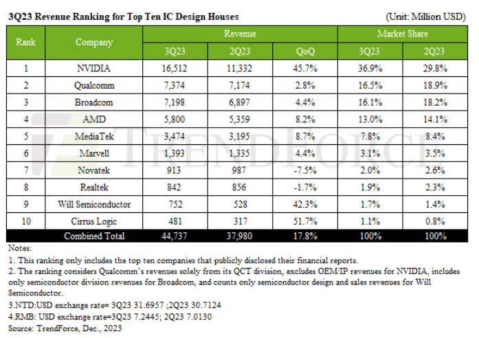
  TrendForce reports that 3Q23 has been a historic quarter for the world’s leading IC design houses as total revenue soared 17.8% to reach a record-breaking US$44.7 billion. This remarkable growth is fueled by a robust season of stockpiling for smartphones and laptops, combined with a rapid acceleration in the shipment of generative AI chips and components. NVIDIA, capitalizing on the AI boom, emerged as the top performer in revenue and market share. Notably, analog IC supplier Cirrus Logic overtook US PMIC manufacturer MPS to snatch the tenth spot, driven by strong demand for smartphone stockpiling.  NVIDIA’s revenue soared 45.7% to US$16.5 billion in the third quarter, bolstered by sustained demand for generative AI and LLMs. Its data center business—accounting for nearly 80% of its revenue—was a key driver in this exceptional growth.  Qualcomm, riding the wave of its newly launched flagship AP Snapdragon 8 Gen 3 and the release of new Android smartphones, saw its third-quarter revenue climb by 2.8% QoQ to around US$7.4 billion. However, NVIDIA’s rapid growth eroded Qualcomm’s market share to 16.5%. Broadcom, with its strategic emphasis on AI server-related products like AI ASIC chips, high-end switches, and network interface cards, along with its seasonal wireless product stockpiling, managed to offset weaker demand in server storage connectivity and broadband. This strategic maneuvering led to a 4.4% QoQ revenue boost to US$7.2 billion.  AMD witnessed an 8.2% increase in its 3Q revenue, reaching US$5.8 billion. This success was due to the widespread adoption of its 4th Gen EPYC server CPUs by cloud and enterprise customers and the favorable impact of seasonal laptop stockpiling. MediaTek's revenue rose by 8.7% to US$3.5 billion in the third quarter, buoyed by a healthy replenishment demand for smartphone APs, WiFi6, and mobile/laptop PMIC components, as inventories across brand clients stabilized.  Cirrus Logic ousts MPS from tenth position thanks to smartphone inventory replenishment  Marvell also made significant gains, with its third-quarter revenue hitting US$1.4 billion, a 4.4% QoQ increase. This growth was primarily driven by increasing demand for generative AI from cloud clients and the expansion of its data center business—despite declines in sectors like enterprise networking and automotive. However, the outlook for some sectors remains mixed, with areas like TV and networking still facing uncertainties, leading to a cautious approach from clients. This resulted in some IC design companies, such as Novatek and Realtek, witnessing a decline in revenues by 7.5% and 1.7%, respectively.  Will Semiconductor benefited from the demand for Android smartphone components, breaking free from past inventory corrections with a 42.3% increase in 3Q revenue to US$752 million. Cirrus Logic, similarly capitalizing on the smartphone component stockpiling trend, saw a significant 51.7% jump in revenue to US$481 million, ousting MPS from the top ten.  In summary, TrendForce forecasts sustained growth for the top ten IC design houses in the upcoming fourth quarter. This optimistic outlook is underpinned by a gradual normalization of inventory levels and a modest seasonal rebound in the smartphone and notebook market. Additionally, the global surge in LLMs extends beyond CSPs, internet companies, and private enterprises, reaching regional countries and small-to-medium businesses, further bolstering this positive revenue trend.
2023-12-22 16:13 阅读量:1820
  • 一周热料
  • 紧缺物料秒杀
型号 品牌 询价
BD71847AMWV-E2 ROHM Semiconductor
MC33074DR2G onsemi
RB751G-40T2R ROHM Semiconductor
TL431ACLPR Texas Instruments
CDZVT2R20B ROHM Semiconductor
型号 品牌 抢购
BP3621 ROHM Semiconductor
STM32F429IGT6 STMicroelectronics
TPS63050YFFR Texas Instruments
BU33JA2MNVX-CTL ROHM Semiconductor
IPZ40N04S5L4R8ATMA1 Infineon Technologies
ESR03EZPJ151 ROHM Semiconductor
热门标签
ROHM
Aavid
Averlogic
开发板
SUSUMU
NXP
PCB
传感器
半导体
相关百科
关于我们
AMEYA360微信服务号 AMEYA360微信服务号
AMEYA360商城(www.ameya360.com)上线于2011年,现 有超过3500家优质供应商,收录600万种产品型号数据,100 多万种元器件库存可供选购,产品覆盖MCU+存储器+电源芯 片+IGBT+MOS管+运放+射频蓝牙+传感器+电阻电容电感+ 连接器等多个领域,平台主营业务涵盖电子元器件现货销售、 BOM配单及提供产品配套资料等,为广大客户提供一站式购 销服务。